TS-7250-V3 DIO Header

From embeddedTS Manuals
Revision as of 15:57, 22 September 2023 by Mark (talk | contribs)

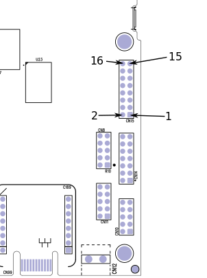
The DIO header is a 0.1" pitch 2x8 header including SPI and GPIO. All pins on this header are 5V tolerant except SPI output pins. The SPI input pins are 5V tolerant and can be connected to a 5V SPI device. All of these DIO include pullups.

Signals Pin Layout
Pin IO Type Signal
1 FPGA 3.3-V LVTTL+QS3861 GPIO Bank 5 IO 1
2 GND
3 FPGA 3.3-V LVTTL+QS3861 GPIO Bank 5 IO 2
4 Open drain[1] Current Sink Output Bank 0 IO 30
5 FPGA 3.3-V LVTTL+QS3861 GPIO Bank 5 IO 3 / ttyS14 TX
6 FPGA 3.3-V LVTTL spidev 4.0 Chip Select / GPIO Bank 5 IO 11
7 FPGA 3.3-V LVTTL+QS3861 GPIO Bank 5 IO 4 / ttyS14 RX
8 FPGA 3.3-V LVTTL+QS3861 GPIO Bank 5 IO 5
9 FPGA 3.3-V LVTTL+QS3861 GPIO Bank 5 IO 6 / ttyS15 TX
10 FPGA 3.3-V LVTTL+QS3861 spidev 4.0 MISO / GPIO Bank 5 IO 10 [2]
11 FPGA 3.3-V LVTTL+QS3861 GPIO Bank 5 IO 7 / ttyS15 RX
12 FPGA 3.3-V LVTTL spidev 4.0 MOSI / GPIO Bank 5 IO 15
13 FPGA 3.3-V LVTTL+QS3861 GPIO Bank 5 IO 8 / ttyS14 TXEN
14 FPGA 3.3-V LVTTL spidev 4.0 CLK / GPIO Bank 5 IO 14
15 FPGA 3.3-V LVTTL+QS3861 GPIO Bank 5 IO 9 / ttyS15 TXEN
16 3.3V

TS-7250-V3-DIO Header.svg

  1. High drives ground, low is tristate.
  2. This pin is input only even when in the GPIO mode
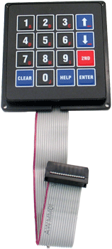
KPAD.jpg

To use the SPI pins on this header as GPIO instead, disable SPI by changing the FPGA Syscon 0x08 bit 10:

​tshwctl -a 0x8 --poke32 0x400

The DIO header is designed to provide compatibility with the KPAD accessory. This is a 4x4 numerical keypad. This is supported in userspace with the keypad.c source code, or the "keypad" utility which is included in the shiping image.

This debounces presses to 50ms, and does not repeat when numbers are held. This will output a string containing the key that is pressed. Eg:

root@tsimx6:~# keypad
1
UP
DOWN
2ND
ENTER