8160-pc104: Difference between revisions
From embeddedTS Manuals
No edit summary |
No edit summary |
||
| Line 20: | Line 20: | ||
You can also drive these DIO to manually manipulate the PC104 address to make peripherals usable that require a higher range of address than provided by the default address space of the MUXBUS. | You can also drive these DIO to manually manipulate the PC104 address to make peripherals usable that require a higher range of address than provided by the default address space of the MUXBUS. | ||
{| | {| | ||
| | |||
{| class=wikitable | {| class=wikitable | ||
! Pin | ! Pin | ||
| Line 186: | Line 187: | ||
| Ground | | Ground | ||
|} | |} | ||
| [[File:TS-8100-PC104 Pinout.png|400px]] | | [[File:TS-8100-PC104 Pinout.png|400px]] | ||
|} | |} | ||
{{Warning|Most of the pins on the PC104 bus are only 3.3V tolerant. Refer to the schematic for more details.}} | {{Warning|Most of the pins on the PC104 bus are only 3.3V tolerant. Refer to the schematic for more details.}} | ||
Revision as of 11:21, 28 March 2013
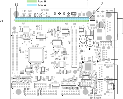
The PC-104 connector consists of two rows of pins labeled A and B, the numbering of of which is shown below. The signals for the PC-104 are generated by the MAX240 PLD located on the baseboard. It converts the MUXBUS signals from the dual 100-pin Macrocontroller interface bus. Pin A1 is nearest to the macrocontroller mounting hole.
Any of the IO on this board labelled DIO_ can be controlled through tsctl as PC104_A/B<pin>, or through manipulation of the registers directly.
# Start tsctl server if it is not already running.
# This only needs to be done once
tsctl --server &

# Lookup the logical DIO mapping of the PC104 header pin A16
eval `tsctl 127.0.0.1 System MapLookup PC104_A16`
# If you run this outside of the eval it will return:
# PC104_A16=138

# Toggle the DIO high and low:
tsctl 127.0.0.1 DIO Set $PC104_A16 high
tsctl 127.0.0.1 DIO Set $PC104_A16 low
You can also drive these DIO to manually manipulate the PC104 address to make peripherals usable that require a higher range of address than provided by the default address space of the MUXBUS.
| WARNING: | Most of the pins on the PC104 bus are only 3.3V tolerant. Refer to the schematic for more details. |
