TS-7180 HD12: Difference between revisions
From embeddedTS Manuals
No edit summary |
No edit summary |
||
| Line 13: | Line 13: | ||
|- | |- | ||
| 2 | | 2 | ||
| RXD_HD1_5V <ref>This is a 5V tolerant TTL UART input.</ref> <ref name=hd12uart>By default, no uart is mapped here. These are remapped through [[#FPGA Registers|fpga reg 308]]. For example, to remap UART8(ttymxc7) run "tshwctl --addr 308 --poke 5"</ref> | | RXD_HD1_5V <ref>This is a 5V tolerant TTL UART input.</ref> <ref name=hd12uart>By default, no uart is mapped here. These are remapped through [[#FPGA Registers|fpga reg 308]]. For example, to remap UART8(/dev/ttymxc7) run "tshwctl --addr 308 --poke 5"</ref> | ||
|- | |- | ||
| 3 | | 3 | ||
Revision as of 11:57, 15 June 2021
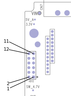
| Signals | Pin Layout | ||||||||||||||||||||||||||
|---|---|---|---|---|---|---|---|---|---|---|---|---|---|---|---|---|---|---|---|---|---|---|---|---|---|---|---|
|
- ↑ This is a 5V tolerant TTL UART input.
- ↑ 2.0 2.1 By default, no uart is mapped here. These are remapped through fpga reg 308. For example, to remap UART8(/dev/ttymxc7) run "tshwctl --addr 308 --poke 5"
