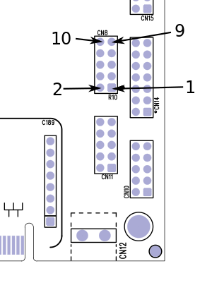
TS-7250-V3 ADC Header: Difference between revisions
From embeddedTS Manuals
No edit summary |
No edit summary |
||
| Line 13: | Line 13: | ||
|- | |- | ||
| 1 | | 1 | ||
| | | iio:device0/voltage0 | ||
|- | |- | ||
| 2 | | 2 | ||
| Line 19: | Line 19: | ||
|- | |- | ||
| 3 | | 3 | ||
| | | iio:device0/voltage1 | ||
|- | |- | ||
| 4 | | 4 | ||
| Line 25: | Line 25: | ||
|- | |- | ||
| 5 | | 5 | ||
| | | iio:device0/voltage5 | ||
|- | |- | ||
| 6 | | 6 | ||
| Line 31: | Line 31: | ||
|- | |- | ||
| 7 | | 7 | ||
| | | iio:device0/voltage8 | ||
|- | |- | ||
| 8 | | 8 | ||
| Line 37: | Line 37: | ||
|- | |- | ||
| 9 | | 9 | ||
| | | iio:device0/voltage9 | ||
|- | |- | ||
| 10 | | 10 | ||
Revision as of 15:19, 6 July 2021
The ADC header supports 5 channels of 0-30VDC ADC. Of these 5, 3 channels support sampling 0-20mA current loops. These channels are sampled from /sys/devices/platform/soc/2100000.aips-bus/2198000.adc/iio:device0#/. See the ADC section for more details on sampling these pins.
| Signals | Pin Layout | ||||||||||||||||||||||
|---|---|---|---|---|---|---|---|---|---|---|---|---|---|---|---|---|---|---|---|---|---|---|---|
|
