TS-7250-V3 MikroBus Header: Difference between revisions
From embeddedTS Manuals
No edit summary |
No edit summary |
||
| Line 21: | Line 21: | ||
|- | |- | ||
| 1 | | 1 | ||
| [[#FPGA_ADC]] | | [[#FPGA_ADC]] / [[#GPIO|GPIO Bank 7 IO 1]] <ref>This signal does not require a mux to use as a GPIO or ADC. To use the ADC signal the GPIO should be an input which is the reset default.</ref> | ||
|- | |- | ||
| 2 | | 2 | ||
| MIKRO_RESET# [[#GPIO|GPIO Bank 7 IO 0]] | | (MIKRO_RESET#) [[#GPIO|GPIO Bank 7 IO 0]] <ref>This signal is pulled high, but your specific click card may require a specific reset duration.</ref> | ||
|- | |- | ||
| 3 | | 3 | ||
Revision as of 09:33, 6 October 2021
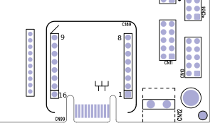
The Mikrobus header is a 0.1" pitch 2x8 header which supports the Mikroe Click board ecosystem. This header features 3.3V, 5V, SPI, GPIO, ADC, PWM, a UART, and PWM. All IO are 3.3V tolerant.
By default all of these headers default to their non-gpio functions. These can be changed in the FPGA syscon register 0x08. For example:
# Make all mikrobus header pins GPIO:
peekpoke 32 0x50004008 0xF0

# Set only SPI to GPIO:
peekpoke 32 0x50004008 0x10
| Signals | Pin Layout | ||||||||||||||||||||||||||||||||||
|---|---|---|---|---|---|---|---|---|---|---|---|---|---|---|---|---|---|---|---|---|---|---|---|---|---|---|---|---|---|---|---|---|---|---|---|
|
