TS-7840: Difference between revisions
No edit summary |
|||
| (71 intermediate revisions by 3 users not shown) | |||
| Line 3: | Line 3: | ||
{{Infobox | {{Infobox | ||
|title = TS-7840 | |title = TS-7840 | ||
|image = https://www. | |image = https://www.embeddedTS.com/images/boards/medium/ts-7840.gif | ||
|titlestyle = | |titlestyle = | ||
|headerstyle = background:#ccf; | |headerstyle = background:#ccf; | ||
|labelstyle = width:33% | |labelstyle = width:33% | ||
|datastyle = | |datastyle = | ||
|data2 = [ | |data2 = [https://www.embeddedTS.com/products/TS-7840 Product Page] | ||
|data3 = [https://www. | |data3 = [https://www.embeddedTS.com/product-images/TS-7840 Product Images] | ||
|data4 = [https://www. | |data4 = [https://www.embeddedTS.com/products/TS-7840?tab=specs Specifications] | ||
|header5 = Documentation | |header5 = Documentation | ||
| | |data9 = [https://files.embeddedTS.com/ts-arm-sbc/ts-7840-linux/ FTP Path] | ||
|header10 = Processor | |header10 = Processor | ||
|data11 = Marvell MV88F6820 | |data11 = Marvell MV88F6820 | ||
|data12 = Armada 385 | |data12 = Armada 385 Arm® Cortex®-A9 800 MHz Dual Core CPU | ||
}} | }} | ||
= Overview = | = Overview = | ||
The TS-7840 is a Single Board Computer (SBC) based on a Marvell MV88F6820 | The TS-7840 is a Single Board Computer (SBC) based on a Marvell MV88F6820 800 MHz Cortex-A9 Dual Core CPU. This board provides 3 independent gigabit Ethernet controllers, including one gigabit port that goes to an onboard switch providing 5 additional PoE capable RJ45 Ethernets that can be use for filtering or switching. | ||
= Getting Started = | = Getting Started = | ||
{{:Generic Getting Started}} | {{:Generic Getting Started}} | ||
== Connect USB Console == | |||
The board includes a USB Type B header connected to the onboard preprogrammed microcontroller. This acts as a USB serial device using the CP210x Virtual COM port. Most operating systems have built-in support for this device, however drivers are available [https://www.silabs.com/products/development-tools/software/usb-to-uart-bridge-vcp-drivers here]. | |||
{{ | {{:Console From Linux Workstation}} | ||
{{:Console from Windows Workstation}} | |||
== Powering up == | |||
The TS-7840 receives power through the 4 pin terminal block (CN4). If a power supply is ordered with the TS-7840 it will include the correct terminal block connected to the power supply. Otherwise the terminal block will ship with the unit. | |||
If | |||
{| class=wikitable | {| class=wikitable | ||
! | ! Pin | ||
! Description | ! Description | ||
|- | |- | ||
| 1 | | 1 | ||
| | | 10-48VDC | ||
|- | |- | ||
| 2 | | 2 | ||
| | | GND | ||
|- | |- | ||
| 3 | | 3 | ||
| | | POE 48VDC | ||
|- | |- | ||
| 4 | | 4 | ||
| | | POE GND | ||
|} | |} | ||
Once power is applied the device will output information via the built in USB console. | |||
The first output is from U-Boot: | |||
= | <pre style="font-family:monospace,Courier New ;background:black; width:18cm; white-space: pre-wrap; white-space: -moz-pre-wrap; word-wrap: break-word; color:white; "> | ||
U-Boot SPL 2017.09-g2bce19ae53 (Aug 26 2019 - 17:13:17) | |||
Detected Device ID 6820 (SAR1 0xCB00230F) | |||
mv_ddr: mv_ddr-armada-17.10.3 | |||
DDR3 Training Sequence - Switching XBAR Window to FastPath Window | |||
DDR Training Sequence - Start scrubbing | |||
DDR3 Training Sequence - End scrubbing | |||
mv_ddr: completed successfully | |||
Trying to boot from MMC1 | |||
force part -> 1 | |||
U-Boot 2017.09-g2bce19ae53 (Aug 26 2019 - 17:13:17 -0700) | |||
SoC: MV88F6820-A0 at 1332 MHz | |||
I2C: ready | |||
DRAM: 2 GiB (666 MHz, ECC enabled) | |||
MMC: mv_sdh: 0 | |||
Model: Technologic Systems TS-7840 | |||
FPGA Base 0xE8000000 | |||
SCSI: MVEBU SATA INIT | |||
SATA link 0 timeout. | |||
AHCI 0001.0000 32 slots 2 ports 6 Gbps 0x3 impl SATA mode | |||
flags: 64bit ncq led only pmp fbss pio slum part sxs | |||
Net: eth2: ethernet@30000, eth3: ethernet@34000, eth1: ethernet@70000 | |||
Press ESC twice to abort autoboot in 3 second(s) | |||
</pre> | |||
{{Note|The "*** Warning - bad CRC, using default environment" can be safely ignored. This indicates that u-boot scripts are not being customized. Typing "env save" will hide these messages, but this is not needed.}} | |||
The | |||
This u-boot and its environment is loaded from the emmc boot partition 0 (/dev/mmcblk0boot0). This a hardware partition that is independent of the main flash on the emmc (/dev/mmcblk0). From here, u-boot will follow u-boots standard Distro boot command. This will check for boot files on the first USB mass storage, then the m.2 SATA, and will by default find a bootable image on eMMC. From here the board will boot to our default [[#Debian]] image. | |||
== First Linux Boot == | |||
When booting with the default settings, a shipped board [[#U-boot Distro Boot|will boot to the eMMC]]. The eMMC by default are pre-programmed with our default [[#Debian|Debian]] 10 Buster image. After Linux boots it will ask the user to log in with a username and password. This uses "root" as the username with no password. This can be changed after logging in with the command "passwd" to set an account password. | |||
From the Linux prompt you can now begin testing out hardware, or beginning your [[#Debian Application Development|application development]]. | |||
== Booting from USB == | |||
{{:TS-7840 Boot over USB}} | |||
= U-Boot = | |||
{{:TS-7840 U-Boot}} | |||
== U-boot Distro Boot == | |||
{{:TS-7840 Uboot Distro Boot}} | |||
= | == U-Boot Environment == | ||
{{:TS-7840 u-boot environment}} | |||
== U-Boot Commands == | |||
{{:TS-7840 u-boot commands}} | |||
{ | |||
== | == U-Boot Development == | ||
{{:TS-7840 U-boot development}} | |||
= Debian 10 = | |||
{{:Debian Buster Description}} | |||
== | == Debian 10 - Getting Started and writing an Image == | ||
{{:TS-7840 Buster Getting started}} | |||
== Debian 10 - Configuring Network == | |||
{{:TS-7840 Buster Network}} | |||
== Debian 10 - Installing New Software == | |||
{{:Buster installing software}} | |||
{{ | == Debian 10 - Setting Up SSH == | ||
{{:Buster setup ssh}} | |||
== | == Debian 10 - Starting Automatically == | ||
{{:Buster Startup Scripts}} | |||
== Debian 10 - Cross Compiling == | |||
{{:Buster armhf cross compile docker}} | |||
== Debian 10 - Backup the image == | |||
{{:Buster Ts-7840 image backup}} | |||
== | == Debian 10 - Compile the Kernel == | ||
{{:Buster Kernel compile}} | |||
= USB Production Imaging Tool = | |||
{{:TS-7840 Production tool}} | |||
= Features = | |||
== Battery Backed RTC == | |||
{{:TS-7840 RTC}} | |||
{{ | == CAN == | ||
{{:TS-7840 CAN}} | |||
== | == CPU == | ||
{{:TS-7840 CPU}} | |||
== | == DDR3 RAM == | ||
{{:TS-7840 ECC}} | |||
== | == eMMC Controller == | ||
{{:TS-7840 eMMC Controller}} | |||
== | == Ethernet == | ||
{{:TS-7840 Ethernet}} | |||
== | === Onboard Marvell Switch Controller === | ||
{{:TS-7840 switch}} | |||
== | === POE Sourcing === | ||
{{:TS-7840 POE Source}} | |||
=== PTP === | |||
{{:TS-7840 PTP}} | |||
== FRAM == | |||
{{:TS-7840 FRAM}} | |||
== FPGA == | |||
{{:TS-7840 FPGA}} | |||
=== FPGA Syscon === | |||
{{:TS-7840 Syscon}} | |||
{ | |||
{ | |||
{{ | === FPGA DIO === | ||
{{:TS-7840 FPGA GPIO Core}} | |||
= | === FPGA 16550 === | ||
{{:TS-7840 16550}} | |||
=== FPGA CAN === | |||
{{:TS-7840 SJA1000}} | |||
=== FPGA SPI === | |||
{{:TS-7840 Opencore SPI}} | |||
=== FPGA ADC === | |||
{{:TS-7840 FPGA ADC}} | |||
== | == GPIO == | ||
{{:TS-7840 GPIO Usage}} | |||
=== FPGA GPIO === | |||
{{:TS-7840 FPGA GPIO}} | |||
== I2C == | |||
{{:TS-7840 I2C}} | |||
== LEDs == | |||
{{:TS-7840 LEDs}} | |||
== PCIe Controller == | |||
{{:TS-7840 PCIe}} | |||
== | == SATA == | ||
{{:TS-7840 SATA}} | |||
== | == Security Chipset (ATSHA204) == | ||
{{:TS-7840 ATSHA204}} | |||
==== | == SPI == | ||
{{:TS-7840 SPI}} | |||
== | == TS-SILO Supercaps == | ||
{{:TS-7840 Supercaps}} | |||
== | == UARTs == | ||
{{:TS-7840 UARTs}} | |||
== | == USB Host == | ||
{{:TS-7840 USB Controller}} | |||
==== | = Specifications = | ||
== I/O Specification == | |||
{{:TS-7840 IO Specs}} | |||
== | == Power Input Specification == | ||
{{:TS-7840 Power supply}} | |||
== Power Consumption == | |||
{{:TS-7840 Power Consumption}} | |||
== | == Power Outputs == | ||
{{:TS-7840 Power Outputs}} | |||
== Thermal Specifications == | |||
{{:TS-7840 Thermal testing}} | |||
==== | = External Interfaces = | ||
== DSL Modem == | |||
{{:TS-7840 DSL Modem}} | |||
=== | === RJ11 === | ||
{{:TS-7840 DSL}} | |||
=== Earth GND connector === | |||
{{:TS-7840 Earth GND}} | |||
== | == Ethernet Interfaces == | ||
{{:TS-7840 Ethernet Interfaces}} | |||
=== | === SFP Ports === | ||
{{:TS-7840 SFP Ports}} | |||
== | == GPS == | ||
{{:TS-7840 GPS}} | |||
== | == Terminal Blocks == | ||
{{:TS-7840 Terminal Block}} | |||
== | == Iridium Modem == | ||
{{:TS-7840 Iridium modem}} | |||
== Jumpers == | |||
{{:TS-7840 Jumpers}} | |||
== Mikrobus == | |||
{{:TS-7840 Mikrobus}} | |||
= | |||
{ | |||
== | === FPGA PWM === | ||
{{:TS-7840 FPGA PWM}} | |||
== Mini PCIe == | |||
{{:TS-7840 minipcie}} | |||
== M.2 SATA == | |||
{{:TS-7840 M2 SATA}} | |||
== | == Nimbelink Socket == | ||
{{:TS-7840 Nimbelink}} | |||
== Power Connector == | |||
{{:TS-7840 Power Connector}} | |||
== | == Push Button == | ||
{{:TS-7840 Push Button}} | |||
== USB Connectors == | |||
{{:TS-7840 USB Connectors}} | |||
== XBEE Header == | |||
{{:TS-7840 XBEE}} | |||
= Revisions and Changes = | = Revisions and Changes = | ||
== | == TS-7840 PCB Revisions == | ||
{{:TS-7840 PCB Revs}} | |||
{ | |||
{ | |||
== | == U-Boot Changelog == | ||
{{:TS-7840 U-boot Changelog}} | |||
== FPGA Changelog == | |||
{{:TS-7840 FPGA Changelog}} | |||
== Software | == Software Images == | ||
=== Debian Changelog === | |||
{{:TS-7840 Debian Changelog}} | |||
= Product Notes = | |||
= | |||
== Trademarks == | |||
{{:Arm Trademark Usage}} | |||
Latest revision as of 12:07, 27 October 2023
| WARNING: | This is PRELIMINARY INFORMATION ONLY. It is certain to change while undergoing editing. |
 | |
| Product Page | |
| Product Images | |
| Specifications | |
| Documentation | |
|---|---|
| FTP Path | |
| Processor | |
| Marvell MV88F6820 | |
| Armada 385 Arm® Cortex®-A9 800 MHz Dual Core CPU |
Overview
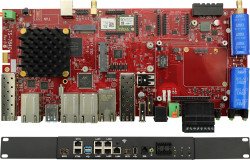
The TS-7840 is a Single Board Computer (SBC) based on a Marvell MV88F6820 800 MHz Cortex-A9 Dual Core CPU. This board provides 3 independent gigabit Ethernet controllers, including one gigabit port that goes to an onboard switch providing 5 additional PoE capable RJ45 Ethernets that can be use for filtering or switching.
Getting Started
A Linux PC is recommended for development. For developers who use Windows, virtualized Linux using VMWare or similar are recommended in order to make the full power of Linux available. The developer will need to be comfortable with Linux anyway in order to work with embedded Linux on the target platform. The main reasons that Linux is useful are:
- Linux filesystems on the microSD card can be accessed on the PC.
- More ARM cross-compilers are available.
- If recovery is needed, a bootable medium can be written.
- A network filesystem can be served.
- Builds such as Linux kernel, buildroot, yocto, distro-seed will not work from WSL1/2 on a case insensitive filesystem.
| WARNING: | Be sure to take appropriate Electrostatic Discharge (ESD) precautions. Disconnect the power source before moving, cabling, or performing any set up procedures. Inappropriate handling may cause damage to the board. |
Connect USB Console
The board includes a USB Type B header connected to the onboard preprogrammed microcontroller. This acts as a USB serial device using the CP210x Virtual COM port. Most operating systems have built-in support for this device, however drivers are available here.
Console from Linux
There are many serial terminal applications for Linux, three common used applications are picocom, screen, and minicom. These examples demonstrate all three applications and assume that the serial device is "/dev/ttyUSB0" which is common for USB adapters. Be sure to replace the serial device string with that of the device on your workstation.
picocom is a very small and simple client.
sudo picocom -b 115200 /dev/ttyUSB0
screen is a terminal multiplexer which happens to have serial support.
sudo screen /dev/ttyUSB0 115200
Or a very commonly used client is minicom which is quite powerful but requires some setup:
sudo minicom -s
- Navigate to 'serial port setup'
- Type "a" and change location of serial device to "/dev/ttyUSB0" then hit "enter"
- If needed, modify the settings to match this and hit "esc" when done:
     E - Bps/Par/Bits          : 115200 8N1
     F - Hardware Flow Control : No
     G - Software Flow Control : No
- Navigate to 'Save setup as dfl', hit "enter", and then "esc"
Console from Windows
Putty is a small simple client available for download here. Open up Device Manager to determine your console port. See the putty configuration image for more details.


Powering up
The TS-7840 receives power through the 4 pin terminal block (CN4). If a power supply is ordered with the TS-7840 it will include the correct terminal block connected to the power supply. Otherwise the terminal block will ship with the unit.
| Pin | Description |
|---|---|
| 1 | 10-48VDC |
| 2 | GND |
| 3 | POE 48VDC |
| 4 | POE GND |
Once power is applied the device will output information via the built in USB console.
The first output is from U-Boot:
U-Boot SPL 2017.09-g2bce19ae53 (Aug 26 2019 - 17:13:17)
Detected Device ID 6820 (SAR1 0xCB00230F)
mv_ddr: mv_ddr-armada-17.10.3
DDR3 Training Sequence - Switching XBAR Window to FastPath Window
DDR Training Sequence - Start scrubbing
DDR3 Training Sequence - End scrubbing
mv_ddr: completed successfully
Trying to boot from MMC1
force part -> 1


U-Boot 2017.09-g2bce19ae53 (Aug 26 2019 - 17:13:17 -0700)

SoC:   MV88F6820-A0 at 1332 MHz
I2C:   ready
DRAM:  2 GiB (666 MHz, ECC enabled)
MMC:   mv_sdh: 0
Model: Technologic Systems TS-7840
FPGA Base 0xE8000000
SCSI:  MVEBU SATA INIT
SATA link 0 timeout.
AHCI 0001.0000 32 slots 2 ports 6 Gbps 0x3 impl SATA mode
flags: 64bit ncq led only pmp fbss pio slum part sxs
Net:   eth2: ethernet@30000, eth3: ethernet@34000, eth1: ethernet@70000
Press ESC twice to abort autoboot in 3 second(s)
| Note: | The "*** Warning - bad CRC, using default environment" can be safely ignored. This indicates that u-boot scripts are not being customized. Typing "env save" will hide these messages, but this is not needed. |
This u-boot and its environment is loaded from the emmc boot partition 0 (/dev/mmcblk0boot0). This a hardware partition that is independent of the main flash on the emmc (/dev/mmcblk0). From here, u-boot will follow u-boots standard Distro boot command. This will check for boot files on the first USB mass storage, then the m.2 SATA, and will by default find a bootable image on eMMC. From here the board will boot to our default #Debian image.
First Linux Boot
When booting with the default settings, a shipped board will boot to the eMMC. The eMMC by default are pre-programmed with our default Debian 10 Buster image. After Linux boots it will ask the user to log in with a username and password. This uses "root" as the username with no password. This can be changed after logging in with the command "passwd" to set an account password.
From the Linux prompt you can now begin testing out hardware, or beginning your application development.
Booting from USB
This board supports booting to an OS image written to a USB drive. This requires a Linux system to write the USB image.
| Note: | This can be run from the board while booted to eMMC, but this should not rewrite the same USB stick that the system has used to boot. Rewriting an image while it is used as the boot media will result in a corrupt image. |
Check lsblk or dmesg to find your USB drive, but the following examples will assume /dev/sdc.
wget http://ftp.embeddedTS.com/ftp/ts-arm-sbc/ts-7840-linux/distributions/debian/tsa38x-debian-buster-latest.tar.xz
sudo sgdisk --zap-all /dev/sdc
sudo sgdisk -n 0:0:0 -t 0:8300 /dev/sdc
sudo mkfs.ext4 /dev/sdc1
sudo mkdir /mnt/usb/
sudo mount /dev/sdc1 /mnt/usb/
sudo tar --numeric-owner -xf tsa38x-debian-buster-latest.tar.xz -C /mnt/usb/
sudo umount /mnt/usb/
If this USB is plugged into USB on startup, it will be chosen instead of the onboard eMMC. For example:
U-Boot 2017.09-gc83820891f (Dec 01 2020 - 15:58:55 -0700)

SoC:   MV88F6820-A0 at 1332 MHz
I2C:   ready
DRAM:  2 GiB (666 MHz, ECC enabled)
MMC:   mv_sdh: 0
** First descriptor is NOT a primary desc on 0:1 **
Model: Technologic Systems TS-7840
FPGA Base 0xE8000000
No MAC programmed to board
SCSI:  MVEBU SATA INIT
SATA link 0 timeout.
AHCI 0001.0000 32 slots 2 ports 6 Gbps 0x3 impl SATA mode
flags: 64bit ncq led only pmp fbss pio slum part sxs
Net:
Warning: ethernet@30000 (eth2) using random MAC address - c2:8f:8e:ad:1e:69
eth2: ethernet@30000
Warning: ethernet@34000 (eth3) using random MAC address - ce:73:52:8c:10:ef
, eth3: ethernet@34000
Warning: ethernet@70000 (eth1) using random MAC address - fe:21:66:02:6d:d7
, eth1: ethernet@70000
Press ESC twice to abort autoboot in 3 second(s)
Unknown command 'tsfpga' - try 'help'
starting USB...
USB0:   USB EHCI 1.00
USB1:   MVEBU XHCI INIT controller @ 0xf10f4000
Register 2000120 NbrPorts 2
Starting the controller
USB XHCI 1.00
USB2:   MVEBU XHCI INIT controller @ 0xf10fc000
Register 2000120 NbrPorts 2
Starting the controller
USB XHCI 1.00
scanning bus 0 for devices... 3 USB Device(s) found
scanning bus 1 for devices... 1 USB Device(s) found
scanning bus 2 for devices... cannot reset port 2!?
2 USB Device(s) found
       scanning usb for storage devices... 1 Storage Device(s) found

Device 0: Vendor: UFD 3.0  Rev: 1100 Prod: Silicon-Power32G
            Type: Removable Hard Disk
            Capacity: 30944.0 MB = 30.2 GB (63373312 x 512)
... is now current device
Scanning usb 0:1...
Found U-Boot script /boot/boot.scr.uimg
643 bytes read in 327 ms (1000 Bytes/s)
root ## Executing script at 00200000
5681664 bytes read in 454 ms (11.9 MiB/s)
23047 bytes read in 307 ms (73.2 KiB/s)
Booting Debian from usb 0:1...
root ## Flattened Device Tree blob at 00100000
   Booting using the fdt blob at 0x100000
   Loading Device Tree to 0fff7000, end 0ffffa06 ... OK

Starting kernel ...

[    1.473899] rtc-ds1307 0-0068: hctosys: unable to read the hardware clock
[    2.084403] EXT4-fs (sda1): couldn't mount as ext3 due to feature incompatibilities
[    2.093073] EXT4-fs (sda1): couldn't mount as ext2 due to feature incompatibilities

Welcome to Debian GNU/Linux 10 (buster)!
U-Boot
U-boot is a bootloader and comes preinstalled on this board. This is loaded in the eMMC hardware boot partitions in /dev/mmcblk0boot0. U-boot sets up the hardware, initializes ECC by scrubbing RAM, and then loads the OS from the available storage devices. Most users will not need to customize u-boot further, and can proceed to the #Debian sections for information on application development.
U-boot Distro Boot
U-boot by default uses u-boots distro bootcmd to determine how to boot. As shipped the board will boot to the preprogrammed eMMC with our #Debian image.
By default this will look at:
| Order | U-boot device name | Description |
|---|---|---|
| 1 | usb0 | First detected USB mass storage device |
| 2 | scsi0 | M.2 SATA port |
| 3 | mmc0 | Onboard eMMC storage |
| 4 | dhcp | DHCP Option [1] |
| 5 | pxe | PXE File [2] |
The default boot order can be left for most users, but boot can be optimized for one boot device by stopping at u-boot and running:
# Boot straight to mmc:
env set boot_targets 'mmc0';
env save

# Boot to usb, then mmc only
env set boot_targets 'usb0 mmc0';
env save

# Set back to default boot order
env set boot_targets 'usb0 scsi0 mmc0 dhcp pxe'
env save
U-boot will search the boot media on either the 1st partition, or if the disk is partitioned with GPT instead of MBR it will search the "bootable" partition. It will then search for these files:
| Order | Search for | Paths | Description |
|---|---|---|---|
| 1 | extlinux | /extlinux/extlinux.conf, /boot/extlinux/extlinux.conf | Menu conf file of kernels |
| 2 | U-boot script | /boot.scr.uimg, /boot.scr, /boot/boot.scr.uimg, /boot/boot.scr | u-boot script with instructions to load the OS |
| 3 | EFI Binary | efi/boot/bootarm.efi | EFI binary (such as grub) |
Our Debian images use a u-boot script in /boot/boot.scr.uimg.
U-Boot Environment
The U-Boot environment on the TS-7840 is stored in the on-board eMMC flash in the /dev/mmcblk0boot0 partition.
# Print all environment variables
env print -a

# Sets the variable bootdelay to 5 seconds
env set bootdelay 5

# Variables can also contain commands
env set hellocmd 'led red on; echo Hello world; led green on;'

# Execute commands saved in a variable
env run hellocmd

# Commit env changes to the spi flash
# Otherwise changes are lost
env save

# Restore env to default
env default -a

# Remove a variable
env delete emmcboot
U-Boot Commands
# The most important command is
help
# This can also be used to see more information on a specific command
help i2c

# Boots into the compressed binary at $loadaddr.
bootz
# Boots into the compressed binary at $loadaddr, specifies the fdtaddr
# so Linux knows where to find the board device-tree
bootz ${loadaddr} - ${fdtaddr}

# Get a DHCP address
dhcp
# This sets ${ipaddr}, ${dnsip}, ${gatewayip}, ${netmask}
# and ${ip_dyn} which can be used to check if the dhcp was successful

# These commands are used for scripting:
false # do nothing, unsuccessfully
true # do nothing, successfully

# This command is used to copy a file from most devices
# Load kernel from SD
load mmc 1:2 ${loadaddr} /boot/zImage
# Load Kernel from eMMC
load mmc 0:2 ${loadaddr} /boot/zImage

# You can view the fdt from u-boot with fdt
load mmc 0:2 $fdtaddr /boot/armada-38x.dtb
fdt addr ${fdtaddr}
fdt print

# You can blindly jump into any memory
# This is similar to bootm, but it does not use the
# u-boot header
load mmc 0:2 ${loadaddr} /boot/custombinary
go ${loadaddr}

# Browse fat,ext2,ext3,or ext4 filesystems:
ls mmc 0:1 /

# Access memory like devmem in Linux, you can read/write arbitrary memory
# using mw and md
# write
mw 0x10000000 0xc0ffee00 1
# read
md 0x10000000 1

# Test memory.
mtest

# The NFS command is like 'load', but used over the network
dhcp
env set serverip 192.168.0.11
nfs ${loadaddr} 192.168.0.11:/path/to/somefile

# Test ICMP
dhcp
ping 192.168.0.11

# Reboot
reset

# Delay in seconds
sleep 10

# You can load HUSH scripts that have been created with mkimage
load mmc 0:1 ${loadaddr} /boot/ubootscript.uimg
source ${loadaddr}

# Most commands have return values that can be used to test
# success, and HUSH scripting supports comparisons like
# test in Bash, but much more minimal
if load mmc 1:1 ${fdtaddr} /boot/zImage;
	then echo Loaded Kernel
else
	echo Could not find kernel
fi

# Commands can be timed with "time"
time bdinfo

# Print U-boot version/build information
version
U-Boot Development
We do provide our u-boot sources, but we do not recommend rebuilding a custom uboot if it can be avoided. We provide our products for as long as possible, and occasionally these require software changes to support replacement components. Often these require no software changes, but if they do we can often update u-boot to add support for a new DDR chipset, or SPI flash without affecting Linux. If your u-boot is customized, it would need to be updated at that time to pull in this support. We will send out a product change notification to anyone who is subscribed to our PCS system when this happens.
Fetch the u-boot sources with:
git clone https://github.com/embeddedTS/u-boot-armada38x.git -b u-boot-2017.09
Download the toolchain here
Install with:
sudo bash poky-glibc-x86_64-meta-toolchain-qt5-cortexa9hf-neon-toolchain-2.2.2.sh
Compile u-boot with:
export ARCH=arm
export CROSS_COMPILE="/opt/poky/2.2.2/sysroots/x86_64-pokysdk-linux/usr/bin/arm-poky-linux-gnueabi/arm-poky-linux-gnueabi-"

make ts7840_defconfig
make -j4
The resulting output file will be "./u-boot-spl.kwb". Copy this file to the TS-7840, and install it on the board with:
echo 0 > /sys/class/block/mmcblk0boot0/force_ro
dd if=u-boot-spl.kwb of=/dev/mmcblk0boot0 conv=fsync
If the system is rendered unbootable by modifying u-boot, this will require an RMA to recover.
Debian 10
Debian is a community run Linux distribution. Debian provides tens of thousands of precompiled applications and services. This distribution is known for stability and large community providing support and documentation. The installation is specific to our board, but most Debian documentation applies:
Debian 10 - Getting Started and writing an Image
Once installed, the default user is "root" with no password.
| Note: | This is a shared image that supports the TS-7820, TS-7825 and TS-7840 |
This image can be written to a USB drive, or to the eMMC. For development, a USB thumbdrive will be simplest. If a bootable USB drive is connected this will take priority over other boot media. Plug in a USB drive and check the last output from "dmesg" to get the USB disk. For example, this may be /dev/sdc.
# Erase all older partitions
sudo sgdisk --zap-all /dev/sdc
# Create one GPT Linux partition
sudo sgdisk -n 0:0:0 -t 0:8300 /dev/sdc
# Create a filesystem and mount
sudo mkfs.ext4 /dev/sdc1
sudo mkdir /mnt/usb/
sudo mount /dev/sdc1 /mnt/usb/
# Extract downloaded image:
sudo tar --numeric-owner -xf ts7840-debian-buster-latest.tar.xz -C /mnt/usb/
sudo chmod 755 /mnt/usb/
sudo umount /mnt/usb/
These commands will also work while booted from a USB drive to rewrite the eMMC. Instead of /dev/sdc you would use /dev/mmcblk0, and instead of /dev/sdc1 you would use /dev/mmcblk0p1.
Debian 10 - Configuring Network
The network in Debian is configured /etc/network/interfaces.d/. For complete documentation, see Debian's documentation here
Some common examples are shown below.
DHCP on eth0:
tee /etc/network/interfaces.d/eth0 <<'EOF' >/dev/null
auto eth0
allow-hotplug eth0
iface eth0 inet dhcp
EOF
Static IP on eth0:
tee /etc/network/interfaces.d/eth0 <<'EOF' >/dev/null
auto eth0
iface eth0 inet static
    address 192.0.2.7/24
    gateway 192.0.2.254
EOF
Debian 10 - Installing New Software
Debian provides the apt-get system which allows management of pre-built applications. The apt tools require a network connection to the internet in order to automatically download and install new software. The update command will download a list of the current versions of pre-built packages.
apt-get update
A common example is installing Java runtime support for a system. Find the package name first with search, and then install it.
root@tsa38x:~# apt-cache search openjdk
default-jdk - Standard Java or Java compatible Development Kit
default-jdk-doc - Standard Java or Java compatible Development Kit (documentation)
default-jdk-headless - Standard Java or Java compatible Development Kit (headless)
default-jre - Standard Java or Java compatible Runtime
default-jre-headless - Standard Java or Java compatible Runtime (headless)
jtreg - Regression Test Harness for the OpenJDK platform
libreoffice - office productivity suite (metapackage)
openjdk-11-dbg - Java runtime based on OpenJDK (debugging symbols)
openjdk-11-demo - Java runtime based on OpenJDK (demos and examples)
openjdk-11-doc - OpenJDK Development Kit (JDK) documentation
openjdk-11-jdk - OpenJDK Development Kit (JDK)
openjdk-11-jdk-headless - OpenJDK Development Kit (JDK) (headless)
openjdk-11-jre - OpenJDK Java runtime, using Hotspot JIT
openjdk-11-jre-headless - OpenJDK Java runtime, using Hotspot JIT (headless)
openjdk-11-jre-zero - Alternative JVM for OpenJDK, using Zero
openjdk-11-source - OpenJDK Development Kit (JDK) source files
uwsgi-app-integration-plugins - plugins for integration of uWSGI and application
uwsgi-plugin-jvm-openjdk-11 - Java plugin for uWSGI (OpenJDK 11)
uwsgi-plugin-jwsgi-openjdk-11 - JWSGI plugin for uWSGI (OpenJDK 11)
uwsgi-plugin-ring-openjdk-11 - Closure/Ring plugin for uWSGI (OpenJDK 11)
uwsgi-plugin-servlet-openjdk-11 - JWSGI plugin for uWSGI (OpenJDK 11)
java-package - Utility for creating Java Debian packages
In this case, the wanted package will likely be the "openjdk-11-jre" package. Names of packages can be found on Debian's wiki pages or the packages site.
With the package name apt-get install can be used to install the prebuilt packages.
apt-get install openjdk-11-jre
# More than one package can be installed at a time.
apt-get install openjdk-11-jre nano vim mplayer
For more information on using apt-get refer to Debian's documentation here.
Debian 10 - Setting Up SSH
Openssh is installed in our default Debian image, but by default openssh does not permit root logins, and requires a password to be set. Additionally, a host key is required if one hasn't already been created on the target board. To allow remote root login:
sed --in-place 's/#PermitRootLogin prohibit-password/PermitRootLogin yes/' /etc/ssh/sshd_config
systemctl restart ssh.service
/bin/ls /etc/ssh/ssh_host*key >/dev/null 2>&1  || ssh-keygen -A
passwd root # Set any password
If you ssh to this system it will now support ssh as root.
Debian 10 - Starting Automatically
A systemd service can be created to start up headless applications. Create a file in /etc/systemd/system/yourapp.service
[Unit]
Description=Run an application on startup

[Service]
Type=simple
ExecStart=/usr/local/bin/your_app_or_script

[Install]
WantedBy=multi-user.target
If networking is a dependency add "After=network.target" in the Unit section. Once you have this file in place add it to startup with:
# Start the app on startup, but will not start it now
systemctl enable yourapp.service

# Start the app now, but doesn't change auto startup
systemctl start yourapp.service
| Note: | See the systemd documentation for in depth documentation on services. |
Debian 10 - Cross Compiling
Debian only provides their cross compiler for their distribution. Our examples will set up a Docker for Debian to use for development. If using Debian 10 Buster directly, or through a VM then the docker usage can be skipped.
Create a file called "Dockerfile" with these contents:
FROM debian:buster

RUN dpkg --add-architecture armhf

RUN apt-get update && apt-get install -y \
    autogen \
    automake \
    bash \
    bc \
    bison \
    build-essential \
    bzip2 \
    ca-certificates \
    ccache \
    chrpath \
    cpio \
    curl \
    diffstat \
    fakeroot \
    file \
    flex \
    gawk \
    gcc-arm-linux-gnueabihf \
    git \
    gzip \
    kmod \
    libgpiod-dev:armhf \
    libncursesw5-dev \
    libssl-dev \
    libtool \
    locales \
    lzop \
    make \
    multistrap \
    ncurses-dev \
    pkg-config \
    python \
    python3 \
    python3-pip \
    python3-pexpect \
    qemu-user-static \
    rsync \
    socat \
    runit \
    texinfo \
    u-boot-tools \
    unzip \
    vim \
    wget \
    xz-utils

# To make a more readable PS1 to show we are in the Docker
ENV debian_chroot debian_buster
RUN echo "PS1='\${debian_chroot}\\[\033[01;32m\\]@\\H\[\\033[00m\\]:\\[\\033[01;34m\\]\\w\\[\\033[00m\\]\\$ '" >> /etc/bash.bashrc

# Set up locales.  Needed by yocto.
RUN sed -i -e 's/# en_US.UTF-8 UTF-8/en_US.UTF-8 UTF-8/' /etc/locale.gen && \
        echo 'LANG="en_US.UTF-8"'>/etc/default/locale && \
        dpkg-reconfigure --frontend=noninteractive locales && \
        update-locale LANG=en_US.UTF-8

ENV LC_ALL en_US.UTF-8
ENV LANG en_US.UTF-8
ENV LANGUAGE en_US.UTF-8
In the same directory as the file named "Dockerfile" run:
docker build --tag armhf-buster-toolchain .
When this has finished the docker can be used with:
docker run --rm -it --volume $(pwd):/work armhf-buster-toolchain bash
This will map the current directory to /work.
At this point the Debian Docker is ready to compile armhf binaries. For example, create a hello world in your home folder at ~/hello.c
#include <stdio.h>
int main(){
    printf("Hello World\n");
}
To compile this enter the docker with:
docker run -it --volume $(pwd):/work armhf-buster-toolchain bash
# Then from the docker:
cd /work/
arm-linux-gnueabihf-gcc hello.c -o hello
Check "file hello" to verify the binary type:
user@host:~/$ file hello
hello: ELF 32-bit LSB pie executable, ARM, EABI5 version 1 (SYSV), dynamically linked, interpreter /lib/ld-linux-armhf.so.3, for GNU/Linux 3.2.0, BuildID[sha1]=8a8cee3341d3ef76ef6796f72d5722ae9d77c8ea, not stripped
This can also be used to develop against dynamic libraries from Debian. The armhf packages can be installed in the Docker. For example, to link against curl:
# Enter the Docker:
docker run -it --volume $(pwd):/work armhf-buster-toolchain bash
cd /work/

apt-get install libcurl4-openssl-dev:armhf
# Download curl's simple.c example
wget https://raw.githubusercontent.com/bagder/curl/master/docs/examples/simple.c
arm-linux-gnueabihf-gcc simple.c -o simple -lcurl
The "simple" binary is now built for armhf and links dynamically to curl.
This will only retain the armhf libcurl package until the docker is exited. To make the changes permanent, add the package to the Dockerfile and rerun:
docker build --tag armhf-buster-toolchain .
Debian 10 - Backup the image
To create backups / restore images, it is recommended to first boot to USB. A disk should not be backed up or written while it is used to boot.
If your image is a single partition it can be backed up as a tar file. This allows the media to easily expand to any disk size.
Create a backup tar
mkdir /mnt/emmc
mount /dev/mmcblk0p1 /mnt/emmc/
tar -cJf /root/backup-of-image.tar.xz -C /mnt/emmc/
umount /mnt/emmc/
Write a tar image to the eMMC
sgdisk --zap-all /dev/mmcblk0
sgdisk -n 0:0:0 -t 0:8300 /dev/mmcblk0
mkfs.ext4 /dev/mmcblk0p1
mkdir /mnt/emmc
mount /dev/mmcblk0p1 /mnt/emmc/
tar -xf /root/backup-of-image.tar.xz -C /mnt/emmc/
umount /mnt/emmc/
The same steps work with SATA, using the SATA device seen in "lsblk". This will be /dev/sda or /dev/sdb depending on the drive.
Debian 10 - Compile the Kernel
The kernel can be compiled on its own using the Debian 10 Cross Compiler. This should be run from a workstation, and not directly on the board. As with the Debian development, this requires setting up the docker for cross compiling.
This process will generate a tar that can be extracted over an image to update the kernel.
Enter the cross compile environment:
# Create a place to store the kernel:
mkdir -p ~/Projects/tsa38x/kernel/
cd ~/Projects/tsa38x/kernel/
docker run -it --volume $(pwd):/work armhf-buster-toolchain bash
Inside the docker run:
git clone https://github.com/embeddedTS/linux-a38x.git --depth 1 -b linux-4.14.y linux-4.14
cd linux-4.14

export ARCH=arm
export CROSS_COMPILE=arm-linux-gnueabihf-

make tsa38x_defconfig

# Make source or config customizations here

export TEMP=$(mktemp -d)
make -j $(nproc --all) all zImage
mkdir "$TEMPDIR/boot/" && \
cp arch/arm/boot/zImage  "$TEMPDIR"/boot/zImage && \
cp arch/arm/boot/dts/armada-385-ts*.dtb "$TEMPDIR"/boot/ && \
INSTALL_MOD_PATH="$TEMPDIR" make modules_install && \
tar czf kernel.tar.gz -C $TEMPDIR . &&
rm -rf $TEMPDIR
After building this will output a kernel to ~/Projects/tsa38x/kernel/linux/kernel.tar.gz. This file can be copied to the board, and then installed with:
tar -xf kernel.tar.gz -C /
This will extract the kernel/modules/firmware over the existing image. On the next boot, the system will use the new kernel.
This can also be added to an tar image with:
mkdir /tmp/image/
sudo tar --numeric-owner -xf old-image.tar.bz2 -C /tmp/image/
sudo tar -xf kernel.tar.gz -C /tmp/image/
sudo tar --numeric-owner -cjf new-image.tar.bz2 -C /tmp/image .
USB Production Imaging Tool
The TS-7840 supports using a USB thumbdrive to rewrite the onboard media. If the USB media is present on startup it will be chosen instead of eMMC. The startup script will:
- Turn on the RED LED
- Rewrite emmc/sd/u-boot as requested
- Blink green to indicate a pass
* Blinking red indicates a failure. See the console output for more details.
Rewriting a full emmc image typically takes around 5-10 minutes depending on the image size.
The blast image and scripts require a minimum of 50 MB; this plus any disk images or tarballs used dictate the minimum disk size required. The USB drive must have at least 1 partition, with the first partition being formatted ext2/3/4 or fat32/vfat.
wget http://ftp.embeddedTS.com/ftp/ts-arm-sbc/ts-7840-linux/usb-blaster/tsa38x-usb-production-rootfs-latest.tar.xz

# This assumes USB drive is /dev/sdc:
sudo mkfs.ext4 /dev/sdc1
sudo mkdir /mnt/usb/
sudo mount /dev/sdc1 /mnt/usb/
sudo tar --numeric-owner -xf /path/to/tsa38x-usb-production-rootfs-latest.tar.xz -C /mnt/usb/
# Copy image files to /mnt/usb/
sudo umount /mnt/usb/
At this point disk images or tarballs would be copied to the /mnt/usb/ folder and named as noted below. The latest disk images we provide can be downloaded from our FTP site, see the backup and restore section for links to these files. Note that the script expects images and tarballs to have specific names. When using an ext* filesystem, symlinks can be used.
The formatted USB drive boots into a small buildroot initramfs environment with filesystem and partitioning tools installed. This can be used to format SD, eMMC, or other disks. The buildroot starts up and calls /blast.sh on the USB device. By default this script is set up to look for a number of of specific files on the USB disk and write to media on the host device. Upon completion of the script the green or red LEDs will blink to visually indicate a pass or fail of the script. This script can be used without modification to write images from USB with these filenames:
| eMMC | emmcimage.tar.xz | Tar of the filesystem. This will repartition the eMMC to 1 ext4 partition and extract this tar to the filesystem. If present, a /md5sums.txt will be checked and every file can be verified on the filesystem. This md5sums file is optional and can be omitted, but it must not be blank if present. |
|---|---|---|
| emmcimage.dd.xz | Disk image of the card. This will be written to mmcblk1 directly. If present a emmcimage.dd.md5 will cause the written data on the eMMC to be read back and verified against this checksum. | |
| SATA | sataimage.tar.xz | Tar of the filesystem. This will repartition the SATA to 1 ext4 partition and extract this tar to the filesystem. If present, a /md5sums.txt will be checked and every file can be verified on the filesystem. This md5sums file is optional and can be omitted, but it must not be blank if present. |
| sataimage.dd.xz | Disk image of the card. This will be written to mmcblk1 directly. If present a emmcimage.dd.md5 will cause the written data on the eMMC to be read back and verified against this checksum. |
Most users should be able to use the above script without modification. Our buildroot sources are available from our github repo with instructions to rebuild this "tsa38x_usbprod_defconfig" target.
Features
Battery Backed RTC
This board includes an onboard battery backed ST M41T00S using an external and replaceable coin cell battery. The RTC is connected to the CPU via I2C and is handled by the kernel, and is presented as a standard RTC device in linux (/dev/rtc0).
The default Debian Linux image will by default pull time from the rtc on startup, and set it each time there is a synchronization with NTP. By default, no manual interaction is needed for the RTC to function, but if needed hwclock is typically used to interface with the RTC.
The RTC ships with an initial synchronization from the factory, but if the battery is shorted or removed during installation in the field it may lose its time.
CAN
The FPGA includes a CAN controller that is compatible with the NXP SJA1000 register set. This driver is accessed using socketcan:
The can-utils package in Debian provides utilities that can be used for testing:
## First, set the baud rate and bring up the device:
ip link set can0 type can bitrate 250000
ip link set can0 up

## Dump data & errors:
candump can0 &

## Send the packet with:
#can_id = 0x7df
#data 0 = 0x03
#data 1 = 0x01
#data 2 = 0x0c
cansend can0 7DF#03010C
The above example packet is designed to work with the Ozen Elektronik myOByDic 1610 ECU simulator to read the RPM speed. In this case, the ECU simulator would return data from candump with:
 <0x7e8> [8] 04 41 0c 60 40 00 00 00
 <0x7e9> [8] 04 41 0c 60 40 00 00 00
In the output above, columns 6 and 7 are the current RPM value. This shows a simple way to prove out the communication before moving to another language.
The following example sends the same packet and parses the same response in C:
#include <stdio.h>
#include <pthread.h>
#include <net/if.h>
#include <string.h>
#include <unistd.h>
#include <net/if.h>
#include <sys/ioctl.h>
#include <assert.h>
#include <linux/can.h>
#include <linux/can/raw.h>

int main(void)
{
	int s;
	int nbytes;
	struct sockaddr_can addr;
	struct can_frame frame;
	struct ifreq ifr;
	struct iovec iov;
	struct msghdr msg;
	char ctrlmsg[CMSG_SPACE(sizeof(struct timeval)) + CMSG_SPACE(sizeof(__u32))];
	char *ifname = "can0";

	if((s = socket(PF_CAN, SOCK_RAW, CAN_RAW)) < 0) {
		perror("Error while opening socket");
		return -1;
	}

	strcpy(ifr.ifr_name, ifname);
	ioctl(s, SIOCGIFINDEX, &ifr);
	addr.can_family  = AF_CAN;
	addr.can_ifindex = ifr.ifr_ifindex;

	if(bind(s, (struct sockaddr *)&addr, sizeof(addr)) < 0) {
		perror("socket");
		return -2;
	}

 	/* For the ozen myOByDic 1610 this requests the RPM guage */
	frame.can_id  = 0x7df;
	frame.can_dlc = 3;
	frame.data[0] = 3;
	frame.data[1] = 1;
	frame.data[2] = 0x0c;

	nbytes = write(s, &frame, sizeof(struct can_frame));
	if(nbytes < 0) {
		perror("write");
		return -3;
	}

	iov.iov_base = &frame;
	msg.msg_name = &addr;
	msg.msg_iov = &iov;
	msg.msg_iovlen = 1;
	msg.msg_control = &ctrlmsg;
	iov.iov_len = sizeof(frame);
	msg.msg_namelen = sizeof(struct sockaddr_can);
	msg.msg_controllen = sizeof(ctrlmsg);
	msg.msg_flags = 0;

	do {
		nbytes = recvmsg(s, &msg, 0);
		if (nbytes < 0) {
			perror("read");
			return -4;
		}

		if (nbytes < (int)sizeof(struct can_frame)) {
			fprintf(stderr, "read: incomplete CAN frame\n");
		}
	} while(nbytes == 0);

	if(frame.data[0] == 0x4)
		printf("RPM at %d of 255\n", frame.data[3]);

	return 0;
}
See the Kernel's CAN documentation here. Other languages have bindings to access CAN such as Python, Java using JNI.
In production use of CAN we also recommend setting a restart-ms for each active CAN port.
ip link set can0 type can restart-ms 100
This allows the CAN bus to automatically recover in the event of a bus-off condition.
CPU
This board features the Marvell Armada 385 88F6820 CPU. This is a dual core Arm Cortex-A9 that runs at 800 MHz.
DDR3 RAM
This board includes 5 onboard ram chips. Of these, 4 provide the 2GB of usable RAM for the OS, and the additional chip provides storage for ECC. ECC is always enabled on this system.
The CPU is capable of autocorrecting single bit failures, and detecting double bit failures. The mvebu_edac driver will report any failures to the kernel log. In the case of a single bit failure:
EDAC MC0: 1 CE MVEBU on mc#0csrow#0channel#0 (csrow:0 channel:0 page:0xc8e offset:0xc8e000 grain:8 syndrome:0x5b99e5 - Single bit ECC Failure)
A double bit failure will print out this message, and also attempt a system reboot.
EDAC MC0: 1 UE MVEBU on mc#0csrow#0channel#0 (csrow:0 channel:0 page:0x8e offset:0x8e000 grain:8 - Double bit ECC Failure)
To have the system not reboot in case of a double bit failure and just report change the kernel cmdline to include "mvebu_edac.edac_reboot_on_fail=0".
eMMC Controller
This board includes a Micron eMMC module. Our off the shelf builds are 4GiB, but up to 64GiB are available for larger builds. The eMMC flash appears to Linux as an SD card at /dev/mmcblk0. Our default programming will include one partition programmed with our Debian image.
The CPU boots out of the emmc's hardware boot partitions /dev/mmcblk0boot0 and /dev/mmcblk0boot1. These are both 16MB, and are separate from the mmcblk0 flash. Erasing or manipulating /dev/mmcblk0 and its partitions will not affect these hardware partitions. The board boots to /dev/mmcblk0boot0 by default, but boot1 can be selected if it has been written with a valid bootloader. This allows atomic updates in the field of u-boot, but should only be done with care as it can leave your board not booting if a bad image is written before switching the active boot partition.
| WARNING: | This may need a development board or RMA to recover the board if the CPU fails to boot. Make certain a valid u-boot is present on a boot device before switching to it. |
Write a u-boot to mmcblk0boot1 with:
echo 0 > /sys/block/mmcblk0boot1/force_ro
dd if=/path/to/u-boot.kwb bs=1M of=/dev/mmcblk0boot1
Once the data has been verified as written, the active boot partition can be switched to mmcblk0boot1:
# The argument after enable should be 2 for mmcblk0boot1, or 1 for mmcblk0boot0
mmc bootpart enable 2 1 /dev/mmcblk0
The active partition can be read as part of the extcsd read:
mmc extcsd read /dev/mmcblk0
Ethernet
The TS-7840 supports 7 total Ethernets. The CPU offers a total of 3 Ethernet ports which each have 1Gb/s of bandwidth available. The eth0/eth1 ports directly provide a connection to a dedicated CPU Ethernet. The eth2 port is connected to a Marvell 88E6352 gigabit switch.

The gigabit switch provides 5 external Ethernet ports. On startup all ports are disabled and Linux configures all 5 ports (lan0-lan4) to forward packets only to and from the CPU Ethernet port. These interfaces will act as individual Ethernet ports, with the exception that they share 1Gb/s to the CPU. If ports are bridged with brctl, the switch will connect their internal VLANs and forward packets between them without requiring the CPU's intervention. The WAN ports can also be forwarded to LAN ports the same with with brctl, but this will use CPU time instead to coordinate bridging the ports.
Onboard Marvell Switch Controller
The Marvell 88E6352 switch is supported by Linux's DSA (Distributed Switch Architecture). On startup Linux will expose all of the external ports as separate Ethernet ports. List all interfaces with:
ip a
The "lan0-lan4" ports on the TS-7840 are the external switch ports. By default these are configured to forward packets between the external port, and the CPU "eth2" interface. Packets will not forward between the external ports unless configured with brctl. To bring up a lan port:
# Bring up eth2, required for any of the switch
# ports to send/receive packets to the CPU
ip link set eth2 up
ip link set lan0 up
# At this point lan0 can be configured like any normal network interface
# Eg, start a dhcp client:
dhclient lan0
The switch can also be configured to connect ports together to pass packets without the CPU's intervention. This is done with brctl. For example, to bridge lan0 and lan1 together:
# Create a bridge interface
brctl addbr br0
# Add interfaces to the bridge
brctl addif br0 lan0
brctl addif br0 lan1

# Bring up the interfaces, note that eth2 is not
# required to be up in order to bridge the ports
# unless packets must be accessed by Linux.
ip link set lan0 up
ip link set lan1 up
# lastly, bring up the bridge
ip link set br0 up
After this bridge is up, to access lan0/lan1 ports the br0 interface should be used. This br0 interface can now be treated like any other interface. Additional bridges can be created with "brctl addbr", and may include any of the externally available network ports.
POE Sourcing
The LAN4 (T1) port supports acting as a POE+ source (25W) to power another device. This requires a 48VDC supply to be connected to the #Power Connector, and enabling the POE source after boot.
# Enable POE Power
gpioset 3 6=0
PTP
FRAM
This platform supports a soldered-down, non-volatile Ferroelectric RAM (FRAM) device. The Cypress FM25L16B is a 2 KiB FRAM device in a configuration not unlike an SPI EEPROM. The nature of FRAM means it is non-volatile, incredibly fast to write, and is specified with 100 trillion read/write cycles (per each of the 256 sequential 8 byte rows) with a 150 year data retention at temperatures below 65 °C. The device is connected to Linux and presents itself as a flat file that can be read and written like any standard Linux file.
The EEPROM file can be found at /sys/class/spi_master/spi2/spi0.0/eeprom, and should be accessed like a normal file to write and read data in the FRAM.
FPGA
The TS-7840 includes an Intel Cyclone IV FPGA. This is connected to the CPU over a x1 PCIe 2.0 lane, and provides additional perihperals and IO expansion to the system.
The onboard FPGA also permits customization such as adding quadrature encoders, PWM, additional serial ports, DMX, or other unique communication protocols. Please contact Technologic Systems if you require custom FPGA logic.
The FPGA registers are in PCIe BAR0 of 1e6d:7840, and use legacy level based interrupts for the shared peripherals.
All FPGA peripherals have drivers in our default BSP, but the FPGA registers can be manually accessed with fpga_peekpoke:
# 0x0 maps to the FPGA syscon, and register 0 of the syscon returns the FPGA revision
fpga_peekpoke 32 0x0
This will return the revision, such as 0x23.
| Offset | Description |
|---|---|
| 0x0 | FPGA Syscon |
| 0x24 | FPGA DIO Bank 0 |
| 0x40 | FPGA DIO Bank 1 |
| 0x5c | FPGA DIO Bank 2 |
| 0xa4 | FPGA RNG |
| 0x100 | 16550 #0 (COM1 RS-232) |
| 0x108 | 16550 #1 (COM2 RS-232) |
| 0x110 | 16550 #2 (GPS) |
| 0x1118 | 16550 #3 (Nimbelink) |
| 0x120 | 16550 #4 (Iridium Modem) |
| 0x128 | 16550 #5 (DSL Modem Debug) |
| 0x130 | 16550 #6 (Mikrobus UART) |
| 0x138 | 16550 #7 (RS-485) |
| 0x140 | 16550 #8 (XBEE) |
| 0x200 | SJA1000 compatible CAN controller |
| 0x400 | SPI controller |
| 0x800 | SDcore |
FPGA Syscon
| Offset | Bits | Access | Description |
|---|---|---|---|
| 0x0 | 31 | Read Only | Development build |
| 30:0 | Read Only | FPGA Revision | |
| 0x4 | 31:0 | Read Only | Unique FPGA Hash |
| 0x8 | 31:0 | N/A | Reserved |
| 0xc | 31:0 | RW | Scratch register |
| 0x10 | 31:5 | N/A | Reserved |
| 4 | Read Only | strap_5_pad | |
| 3 | Read Only | strap_4_pad | |
| 2 | Read Only | strap_3_pad | |
| 1 | Read Only | strap_2_pad | |
| 0 | Read Only | strap_1_pad | |
| 0x14 | 31:0 | N/A | Reserved |
| 0x18 | 31 | N/A | Reserved |
| 0x1c | 31:0 | N/A | Reserved |
| 0x20 | 31:0 | N/A | Reserved |
| 0x24 | 31:0 | N/A | Reserved |
| 0x28 | 31:0 | N/A | Reserved |
| 0x2c | 31:0 | N/A | Reserved |
| 0x30 | 31:0 | N/A | Reserved |
| 0x34 | 31:0 | N/A | Reserved |
| 0x38 | 31:0 | N/A | Reserved |
| 0x3c | 31:0 | N/A | Reserved |
| 0xa4 | 31:0 | Read Only | FPGA RNG |
FPGA DIO
This FPGA includes two banks of GPIO with atomic set/clr for data and output enable, as well as level based IRQs. Under Linux this is exposed as /dev/gpiochip2 and /dev/gpiochip3. These character devices are normally accessed with libgpiod. The utilities from libgpiod are included in our shipping image and allow accessing GPIO from the shell prompt.
See gpioinfo for a list of all usable GPIO:
gpioinfo /dev/gpiochip2 /dev/gpiochip3 /dev/gpiochip4
Returns:
gpiochip2 - 32 lines:
	line   0:  "uart0_irq"       unused   input  active-high
	line   1:  "uart1_irq"       unused   input  active-high
	line   2:  "uart2_irq"       unused   input  active-high
	line   3:  "uart3_irq"       unused   input  active-high
	line   4:  "uart4_irq"       unused   input  active-high
	line   5:  "uart5_irq"       unused   input  active-high
	line   6:  "uart6_irq"       unused   input  active-high
	line   7:  "uart7_irq"       unused   input  active-high
	line   8:  "uart8_irq"       unused   input  active-high
	line   9:      unnamed       unused   input  active-high
	line  10:    "can_irq"       unused   input  active-high
	line  11:    "spi_irq"  "interrupt"   input  active-high [used]
	line  12:      unnamed       unused   input  active-high
	line  13:      unnamed       unused   input  active-high
	line  14:   "sdio_irq"       unused   input  active-high
	line  15:    "sd_busy"       unused   input  active-high
	line  16: "power_fail_3v_pad" unused input active-high
	line  17: "detect_9478_pad" unused input active-high
	line  18: "cpu_access_fpga_flash" unused input active-high
	line  19: "magjack_1_led_padn" "right-green-led" output active-low [used]
	line  20: "blu_led_padn" "right-red-led" output active-low [used]
	line  21: "right_grn_led_padn" "middle-green-led" output active-low [used]
	line  22: "right_red_led_padn" "middle-yellow-led" output active-low [used]
	line  23: "middle_grn_led_padn" "left-green-led" output active-low [used]
	line  24: "middle_yel_led_padn" "left-yellow-led" output active-low [used]
	line  25: "left_grn_led_padn" unused input active-high
	line  26: "left_yel_led_padn" "phy-0-led" output active-low [used]
	line  27:  "bt_en_pad"       unused   input  active-high
	line  28: "wifi_en_pad" unused output active-high
	line  29: "prog_silab_clk_padn" unused input active-high
	line  30: "prog_silab_data_pad" unused input active-high
	line  31: "cpu_push_sw_padn" unused input active-high
gpiochip3 - 32 lines:
	line   0:   "DIG_IO_1"       unused   input  active-high
	line   1:   "DIG_IO_2"       unused   input  active-high
	line   2:   "DIG_IO_3"       unused   input  active-high
	line   3: "en_hs_sw_pad" unused input active-high
	line   4: "mikro_pwm_pad" unused input active-high
	line   5: "dio_fault_3v_padn" unused input active-high
	line   6: "en_poe_padn" unused input active-high
	line   7: "i2c_poe_clk_pad" "scl" input active-high [used]
	line   8: "i2c_poe_dat" "sda" input active-high [used]
	line   9: "spi_0_fpga_cs3_pad" unused input active-high
	line  10: "cage1_sda_pad" "sda" input active-high [used]
	line  11: "cage1_scl_pad" "scl" input active-high [used]
	line  12: "cage1_present_padn" unused input active-high
	line  13: "cage2_present_padn" unused input active-high
	line  14: "cage2_sda_pad" "sda" input active-high [used]
	line  15: "cage2_scl_pad" "scl" input active-high [used]
	line  16: "en_nimbel_4v_pad" unused input active-high
	line  17: "en_nimbel_3v3_pad" unused input active-high
	line  18: "en_emmc_3v3_pad" unused input active-high
	line  19: "en_modem_5v_pad" unused input active-high
	line  20: "en_usb_5v_pad" unused output active-high
	line  21: "disable_nim_usb_pad" unused input active-high
	line  22: "mini_pcie_reset_padn" unused output active-high
	line  23: "ssd_present_padn" unused input active-high
	line  24: "en_xbee_usb_padn" unused input active-high
	line  25: "aux_i2c_dat_pad" "sda" input active-high [used]
	line  26: "aux_i2c_clk_pad" "scl" input active-high [used]
	line  27:      unnamed       unused   input  active-high
	line  28:      unnamed       unused   input  active-high
	line  29:      unnamed       unused   input  active-high
	line  30:      unnamed       unused   input  active-high
	line  31:      unnamed       unused   input  active-high
gpiochip4 - 32 lines:
	line   0: "ird_network_rdy_pad" unused input active-high
	line   1: "ird_modem_on_pad" unused input active-high
	line   2: "eth_100_act_padn" unused input active-high
	line   3: "eth_100_speed_padn" unused input active-high
	line   4: "ssd_act_padn" unused input active-high
	line   5: "mini_sr_latch_pad" unused input active-high
	line   6:      unnamed       unused   input  active-high
	line   7:      unnamed       unused   input  active-high
	line   8:      unnamed       unused   input  active-high
	line   9:      unnamed       unused   input  active-high
	line  10: "mikro_int_pad" unused input active-high
	line  11: "mikro_reset_padn" unused input active-high
	line  12: "mikro_an_3v_pad" unused input active-high
	line  13: "mikro_i2c_clk_pad" "scl" input active-high [used]
	line  14: "mikro_i2c_dat_pad" "sda" input active-high [used]
	line  15: "alt_mikro_pwm_pad" unused input active-high
	line  16: "mikro_an_pwm_pad" unused input active-high
	line  17:   "comp_pad"       unused   input  active-high
	line  18: "mikro_180_pad" unused input active-high
	line  19: "en_mini_5v_pad" unused input active-high
	line  20: "magjack_0_led_padn" "phy-1-led" output active-low [used]
	line  21: "hd10_2_pad"       unused   input  active-high
	line  22: "hd10_4_pad"       unused   input  active-high
	line  23: "hd10_5_pad"       unused   input  active-high
	line  24: "hd10_6_pad"       unused   input  active-high
	line  25: "hd10_8_pad"       unused   input  active-high
	line  26:   "jp1_padn"       unused   input  active-high
	line  27:   "jp2_padn"       unused   input  active-high
	line  28:      unnamed       unused   input  active-high
	line  29:      unnamed       unused   input  active-high
	line  30:      unnamed       unused   input  active-high
	line  31:      unnamed       unused   input  active-high
From here, commands such as gpioget and gpioset can be used:
gpioget /dev/gpiochip2 31 # Get cpu_push_sw_padn
# Returns 1 when not pressed, 0 when pressed

gpioset /dev/gpiochip3 21=0 # Set en_usb_5v_pad to 0, turning off USB 5V
gpioset /dev/gpiochip3 21=1 # Re-enable USB
These driver interfaces should be used in most cases, but the register documentation is provided for driver writers or for those with reasons to go directly to the hardware:
|
|
FPGA 16550
The TS-7840 includes a National Semiconductor 16550A compatible register interface for accessing the FPGA based UARTs. These must be accessed a byte at a time. These use GPIO IRQs from bank0.
By default these UARTs have a crystal of 1.8432MHz. The max baud rate of a 16550 is the input frequency / 16. With the default 1.8432MHz clock this allows typical baud rates of 115200 to 300 baud. There is a command included in our BSP set_uart_baud which can set custom clocks. For example, to use 3MBaud on ttyS1:
root@tsa38x:~# set_uart_baud -p 0 --baud 3000000
port=0
requested_baud=3000000
actual_baud=3000000.000000
baud_ppm_error=823999
This was able to meet the 3M baud rate with minimal ppm error. In your application code, you would tell Linux to use 115200 baud. This will select a divide by 1 for the new clock rate and get 3000000 baud.
If you were to use an unusual baud rate this will print the closest actual_baud rate the clock is capable of reaching. Even if the actual_baud rate is different, as long as the difference between the two devices is < 10% they will typically still be able to communicate.
The 16550s already have existing drivers in our BSP, but the registers are accessible here:
| PCIe BAR0 Offset | UART | IRQ GPIO |
|---|---|---|
| 0x80 | ttyS1 | FPGA GPIO Bank 0 IO 0 |
| 0x88 | ttyS2 | FPGA GPIO Bank 0 IO 1 |
| 0x90 | ttyS3 | FPGA GPIO Bank 0 IO 2 |
| 0x98 | ttyS4 | FPGA GPIO Bank 0 IO 3 |
| 0xa0 | ttyS5 | FPGA GPIO Bank 0 IO 4 |
| 0xa8 | ttyS6 | FPGA GPIO Bank 0 IO 5 |
| 0xb0 | ttyS7 | FPGA GPIO Bank 0 IO 6 |
| 0xb8 | ttyS8 | FPGA GPIO Bank 0 IO 7 |
| 0xc0 | ttyS9 | FPGA GPIO Bank 0 IO 8 |
FPGA CAN
This FPGA includes a SJA1000 compatible controller. The Linux BSP includes a socketcan compatible driver.
See the Kernel's CAN documentation here.
This board comes preinstalled with can-utils. These can be used to communicate over a CAN network without writing any code. The candump utility can be used to dump all data on the network
## First, set the baud rate and bring up the device:
ip link set can0 type can bitrate 250000
ip link set can0 up

## Dump data & errors:
candump can0 &

## Send the packet with:
#can_id = 0x7df
#data 0 = 0x3
#data 1 = 0x1
#data 2 = 0x0c
cansend can0 -i 0x7Df 0x3 0x1 0x0c
## Some versions of cansend use a different syntax.  If the above
## commands gives an error, try this instead:
#cansend can0 7DF#03010C
The above example packet is designed to work with the Ozen Elektronik myOByDic 1610 ECU simulator to read the RPM speed. In this case, the ECU simulator would return data from candump with:
 <0x7e8> [8] 04 41 0c 60 40 00 00 00
 <0x7e9> [8] 04 41 0c 60 40 00 00 00
In the output above, columns 6 and 7 are the current RPM value. This shows a simple way to prove out the communication before moving to another language.
The following example sends the same packet and parses the same response in C:
#include <stdio.h>
#include <pthread.h>
#include <net/if.h>
#include <string.h>
#include <unistd.h>
#include <net/if.h>
#include <sys/ioctl.h>
#include <assert.h>
#include <linux/can.h>
#include <linux/can/raw.h>

int main(void)
{
	int s;
	int nbytes;
	struct sockaddr_can addr;
	struct can_frame frame;
	struct ifreq ifr;
	struct iovec iov;
	struct msghdr msg;
	char ctrlmsg[CMSG_SPACE(sizeof(struct timeval)) + CMSG_SPACE(sizeof(__u32))];
	char *ifname = "can0";

	if((s = socket(PF_CAN, SOCK_RAW, CAN_RAW)) < 0) {
		perror("Error while opening socket");
		return -1;
	}

	strcpy(ifr.ifr_name, ifname);
	ioctl(s, SIOCGIFINDEX, &ifr);
	addr.can_family  = AF_CAN;
	addr.can_ifindex = ifr.ifr_ifindex;

	if(bind(s, (struct sockaddr *)&addr, sizeof(addr)) < 0) {
		perror("socket");
		return -2;
	}

 	/* For the ozen myOByDic 1610 this requests the RPM guage */
	frame.can_id  = 0x7df;
	frame.can_dlc = 3;
	frame.data[0] = 3;
	frame.data[1] = 1;
	frame.data[2] = 0x0c;

	nbytes = write(s, &frame, sizeof(struct can_frame));
	if(nbytes < 0) {
		perror("write");
		return -3;
	}

	iov.iov_base = &frame;
	msg.msg_name = &addr;
	msg.msg_iov = &iov;
	msg.msg_iovlen = 1;
	msg.msg_control = &ctrlmsg;
	iov.iov_len = sizeof(frame);
	msg.msg_namelen = sizeof(struct sockaddr_can);
	msg.msg_controllen = sizeof(ctrlmsg);
	msg.msg_flags = 0;

	do {
		nbytes = recvmsg(s, &msg, 0);
		if (nbytes < 0) {
			perror("read");
			return -4;
		}

		if (nbytes < (int)sizeof(struct can_frame)) {
			fprintf(stderr, "read: incomplete CAN frame\n");
		}
	} while(nbytes == 0);

	if(frame.data[0] == 0x4)
		printf("RPM at %d of 255\n", frame.data[3]);

	return 0;
}
See the Kernel's CAN documentation here. Other languages have bindings to access CAN such as Python, Java using JNI.
In production use of CAN we also recommend setting a restart-ms for each active CAN port.
ip link set can0 type can restart-ms 100
This allows the CAN bus to automatically recover in the event of a bus-off condition.
FPGA SPI
The FPGA includes the opencore SPI controller that is supported by a Linux driver ocspi as "opencores,spi-oc". This SPI bus connects only to the onboard #FRAM chipset. Most users should be able to use this driver as is.
The SPI controller is at FPGA BAR0 + 0x400, has a 50MHz input clock, and follows the documentation here.
FPGA ADC
The TS-7840 includes a simple low speed ADC to support the analog input on mikrobus modules.
- 305hz sample rate
- 8-bits resolution
- 10kohm input impedance
- 0-6V input range
- 3% absolute accuracy
This ADC is accessed using the IIO subsystem. One time samples can be read from /sys/:
root@tsimx6:~# cat /sys/bus/iio/devices/iio\:device0/in_voltage0_raw
127
root@tsimx6:~# cat /sys/bus/iio/devices/iio\:device0/in_voltage0_scale
25.781250000
The raw value is 0-255, and the scale value converts this to real world values. For example, 127*25.78125=3274.21875mV.
Faster samples, up to 305hz, are available using the buffer interface.
root@tsimx6:~# echo 1 > /sys/bus/iio/devices/iio\:device0/scan_elements/in_voltage0_en
root@tsimx6:~# iio_readdev iio:device0 | hexdump -C
WARNING: High-speed mode not enabled
00000000  80 00 00 00 00 00 00 00  4c a8 d9 e8 b7 33 83 15  |........L....3..|
00000010  7f 00 00 00 00 00 00 00  df 8f 22 e9 b7 33 83 15  |.........."..3..|
00000020  7f 00 00 00 00 00 00 00  b7 aa 55 e9 b7 33 83 15  |..........U..3..|
00000030  80 00 00 00 00 00 00 00  e9 d7 86 e9 b7 33 83 15  |.............3..|
In this case, column 1 that starts with 80 is the ADC value. Columns 2-8 are 0 padding. Columns 9-16 are the 64-bit ns timestamp. This is accurate to approximately 10us.
The ADC buffers can also be filled using libiio directly:
#include <stdbool.h>
#include <stdint.h>
#include <string.h>
#include <signal.h>
#include <stdio.h>
#include <assert.h>
#include <inttypes.h>
#include <iio.h>

static bool stop;
static void handle_sig(int sig)
{
	stop = true;
}

int main (int argc, char **argv)
{
	const struct iio_data_format *fmt;
	static struct iio_context *ctx;
	static struct iio_buffer *rxbuf;
	struct iio_channel *chn;
	struct iio_device *dev;

	/* Catch ctrl+c */
	signal(SIGINT, handle_sig);

	ctx = iio_create_default_context();
	assert(ctx);

	iio_context_set_timeout(ctx, 10000);

	assert(iio_context_get_devices_count(ctx) > 0);
	dev = iio_context_find_device(ctx, "e0300900.adc");
	assert(dev);

	chn = iio_device_get_channel(dev, 0); /* voltage0 */
	assert(chn);

	iio_channel_enable(chn);
	fmt = iio_channel_get_data_format(chn);
	assert(fmt);

	rxbuf = iio_device_create_buffer(dev, 256, false);
	assert(rxbuf);

	printf("%s\n", iio_channel_get_id(chn));
	while (!stop) {
		ssize_t nbytes;
		uint8_t *dat;

		nbytes = iio_buffer_refill(rxbuf);
		if (nbytes < 0) {
			printf("Error refilling buf %d\n",(int) nbytes);
			break;
		}
		for (dat = iio_buffer_first(rxbuf, chn);
			dat < (uint8_t *)iio_buffer_end(rxbuf);
			dat += iio_buffer_step(rxbuf)) {
			printf("%d\n", dat[0]);
			//printf("%.0f,\n", (float)dat[0] * fmt->scale);
		}
	}

	iio_buffer_destroy(rxbuf);
	iio_channel_disable(chn);
	iio_context_destroy(ctx);

	return 0;
}
For most users we recommend using the existing linux drivers, but the hardware core can be found at FPGA PCIE BAR0 + 0x900. It is a single 32-bit register:
| Bits | Reset value | Description |
|---|---|---|
| 31:24 | 0x55 | Reserved |
| 23:16 | 0x0 | sample |
| 15:3 | 0x0 | Reserved |
| 2 | 0 | sample_missed [1] |
| 1 | 0 | sample_ready [2] |
| 0 | 1 | standby_en |
GPIO
The Armada 385 and FPGA GPIO are exposed using a kernel character device. This interface provides a set of files and directories for interacting with GPIO which can be used from any language that interact with special files in linux using ioctl() or similar. For our platforms, we pre-install the "libgpiod" library and binaries. Documentation on these tools can be found here. This section only covers using these userspace tools and does not provide guidance on using the libgpiod library in end applications. Please see the libgpiod documentation for this purpose.
A user with suitable permissions to read and write /dev/gpiochip* files can immediately interact with GPIO pins. For example, to read the push switch:
gpioget 2 31
Multiple pins in the same chip can be read simultaneously by passing multiple pin numbers separated by spaces.
To write to a pin, the 'gpioset' command is used. For example, to set mikro_int_pad:
gpioset 3 26=0
Multiple pins in the same chip can be set simultaneously by passing multiple pin=value pairs separated by spaces.
If a call with 'gpioset' or 'gpioget' fails with "Device or resource busy," that means that specific GPIO is claimed by another device. The command 'cat /sys/kernel/debug/gpio' can be used to get a list of all of the system GPIO and what has claimed them.
FPGA GPIO
| Chip | Pin | Net | Description |
|---|---|---|---|
| 2 | 0 | uart0_irq | FPGA internal |
| 2 | 1 | uart1_irq | FPGA internal |
| 2 | 2 | uart2_irq | FPGA internal |
| 2 | 3 | uart3_irq | FPGA internal |
| 2 | 4 | uart4_irq | FPGA internal |
| 2 | 5 | uart5_irq | FPGA internal |
| 2 | 6 | uart6_irq | FPGA internal |
| 2 | 7 | uart7_irq | FPGA internal |
| 2 | 8 | uart8_irq | FPGA internal |
| 2 | 9 | gps_pps | PPS signal from onboard GPS |
| 2 | 10 | can_irq | FPGA internal |
| 2 | 11 | NC | NC |
| 2 | 12 | NC | NC |
| 2 | 13 | NC | NC |
| 2 | 14 | NC | NC |
| 2 | 15 | NC | NC |
| 2 | 16 | NC | NC |
| 2 | 17 | NC | NC |
| 2 | 18 | NC | NC |
| 2 | 19 | NC | NC |
| 2 | 20 | NC | NC |
| 2 | 21 | NC | NC |
| 2 | 22 | ird_network_rdy_pad | CN8 pin 19 |
| 2 | 23 | ird_modem_on_pad | CN8 pin 5 |
| 2 | 24 | oled_i2c_dat_pad | CN13 pin 1 |
| 2 | 25 | oled_i2c_clk_pad | CN13 pin 2 |
| 2 | 26 | grn_led_padn | LED1 |
| 2 | 27 | red_led_padn | LED1 |
| 2 | 28 | blu_led_pad | LED2 |
| 2 | 29 | prog_silab_clk_padn | Onboard Silabs |
| 2 | 30 | prog_silab_data_pad | Onboard Silabs |
| 2 | 31 | cpu_push_sw_padn | SW1 |
| 3 | 0 | en_ls_out_1_pad | CN17 top pin 7 |
| 3 | 1 | en_ls_out_2_pad | CN17 top pin 8 |
| 3 | 2 | en_ls_out_3_pad | CN17 bottom bin 15 |
| 3 | 3 | en_hs_sw_pad | CN17 bottom pin 16 |
| 3 | 4 | mikro_pwm_pad | CN12 pin 16 |
| 3 | 5 | nimbel_pwr_on_pad | Controls open drain output on pin 20 of CN16 [1] |
| 3 | 6 | en_poe_padn | Onboard POE |
| 3 | 7 | i2c_poe_clk_pad | Onboard POE |
| 3 | 8 | i2c_poe_dat_in_pad | Onboard POE |
| 3 | 9 | i2c_poe_dat_out_pad | Onboard POE |
| 3 | 10 | cage1_sda_pad | Onboard SFP K3 |
| 3 | 11 | cage1_scl_pad | Onboard SFP K3 |
| 3 | 12 | cage1_present_padn | Onboard SFP K3 |
| 3 | 13 | cage2_present_padn | Onboard SFP K2 |
| 3 | 14 | cage2_sda_pad | Onboard SFP K2 |
| 3 | 15 | cage2_scl_pad | Onboard SFP K2 |
| 3 | 16 | en_nimbel_4v_pad | Onboard |
| 3 | 17 | en_nimbel_3v3_pad | Enable 3.3V to nimbelink header |
| 3 | 18 | en_emmc_3v3_pad | Enable onboard eMMC power |
| 3 | 19 | en_modem_5v_pad | Enables power to ADSL modem, Internal USB, and Iridium Modem |
| 3 | 20 | en_usb_5v_pad | Enable USB 5V to USB headers |
| 3 | 21 | en_nim_usb_padn | Enables USB to the Nimbelink socket |
| 3 | 22 | mini_pcie_reset_padn | J4 pin 22 |
| 3 | 23 | ssd_present_padn | K6 pin 1 |
| 3 | 24 | en_xbee_usb_padn | Enable USB port on XBEE socket |
| 3 | 25 | mikro_int_pad | CN12 pin 15 |
| 3 | 26 | mikro_reset_pad | CN12 pin 2 |
| 3 | 27 | mikro_an_3v_pad | CN12 pin 1 |
| 3 | 28 | aux_i2c_dat_pad | Mikrobus I2C |
| 3 | 29 | aux_i2c_clk_pad | Mikrobus I2C |
| 3 | 30 | phy_0_led_pad | T2 bottom left LED |
| 3 | 31 | phy_1_led_pad | T2 top left LED |
I2C
This system includes 3 I2C busses.
The first bus is used for the RTC, onboard supervisory microcontroller, and connects to the FPGA.
| Address | Device |
|---|---|
| 0x54 | Onboard Supervisory microcontroller |
| 0x68 | ST M41T00S RTC |
The second bus is used for the security chipset, and the Mikrobus socket
| Address | Device |
|---|---|
| 0x64 | ATSHA204 Security chipset |
The third bus is for the SFP port (K3_A) on the right of the enclosure.
| Address | Device |
|---|---|
| 0x50 | SFP "eeprom" module |
The fourth bus is for the second SFP port (K2_A) on the left edge of the enclosure.
| Address | Device |
|---|---|
| 0x50 | SFP "eeprom" module |
LEDs
The TS-7840 has 6 external status LEDs, one internal blue LED, and control over the link status LEDs on the RJ45.
On startup, U-boot will turn on the left red LED, and turn off all other LEDs. When Linux starts up, it will by default turn the left red LED off, and the left green LED will act as a kernel heartbeat which will blink at rates depending on the system load.
The following LEDs are available on this system:
| LED | Linux Behavior |
|---|---|
| right-green-led | heartbeat trigger |
| right-red-led | Off |
| middle-yellow-led | Off |
| middle-green-led | Off |
| left-green-led | Off |
| left-yellow-led | Off |
| blu-led | Off |
| phy-0-led | f1072004.mdio-mii:00:1Gbps trigger [2] |
| phy-1-led | f1072004.mdio-mii:01:1Gbps trigger [2] |
These are accessed by writing to files:
# On
echo 1 > /sys/class/leds/right-red-led/brightness
# Off
echo 0 > /sys/class/leds/right-red-led/brightness
A number of triggers are also available, including timers, disk activity, and heartbeat. These allow the LEDs to represent various system activities as they occur. See the kernel LED documentation for more information on triggers and general use of LED class devices.
PCIe Controller
The Marvell Armada 385 supports two PCIe 2.0 channels with 1 lane each. On the TS-7840 the onboard FPGA provides all of its peripherals over one of the PCIe lanes. See the #FPGA section for more details on the FPGA's PCIe access.
The other PCIe bus is a x1 lane which is accessible on the #Mini PCIe header.
SATA
The TS-7840 provides one m.2 connector with SATA 3.
SATA disks will appear in Linux as /dev/sda. This is also a possible boot device if a valid operating system is installed on the disk.
Security Chipset (ATSHA204)
The ATSHA204 is an i2c security device that provides:
- 512 bits of OTP Memory. This can be written only once, and read many times,
- Secure key storage for 16x 256-bit keys
- Unique 72-bit serial number
- Internal RNG
On the TS-7840 this is accessed on /dev/i2c-5 at 0x64.
SPI
The CPU includes one SPI controller which has an externally accessible SPI bus on the #Mikrobus header. This is available at /dev/spidev0.1.
See the kernel spidev documentation for more information on interfacing with the SPI peripherals.
TS-SILO Supercaps
UARTs
The TS-7840 includes 9 UARTs for onboard and offboard peripherals.
While /dev/ttyS0 is built into the CPU, the remaining UARTs are 16550As in the FPGA. These operate as standard 16550 compatible UARTs, except they are modified to support an automatically transmit enable. This is used with RS-485 UARTs which will automatically assert TX_EN and deassert RX_EN for the duration of any transmit.
All of these UARTs are accessed using the standard /dev/ interfaces. See these resources for information on programming with UARTs in Linux.
| UART | Type | TXD (+)Location | RXD (-)Location |
|---|---|---|---|
| /dev/ttyS0 | USB | Silabs console board (CN7) | Silabs console board (CN7) |
| /dev/ttyS1 | RS-232 | Terminal block bottom pin 3 | Terminal block bottom pin 2 |
| /dev/ttyS2 | RS-232 | Terminal block bottom pin 5 | Terminal block bottom pin 4 |
| /dev/ttyS3 | Onboard to GPS | N/A | GPS |
| /dev/ttyS4 | 3.3V TTL | Nimbelink CN16 pin 3 | Nimbelink CN16 pin 2 |
| /dev/ttyS5 | 3.3V TTL | Iridium CN8 pin 6 | Iridium CN8 pin 7 |
| /dev/ttyS6 | 3.3V TTL | ADSL CN15 pin 9 | ADSL CN15 pin 8 |
| /dev/ttyS7 | 3.3V TTL | Mikrobus CN12 pin 13 | Mikrobus CN12 pin 14 |
| /dev/ttyS8 | RS-485 | Terminal block top pin 3 | Terminal block top pin 2 |
| /dev/ttyS9 | 3.3V TTL | XBEE CN20 pin 3 | XBEE CN20 pin 2 |
USB Host
The TS-7840 has 3 external USB host ports, and one internal. The dual high external USB supports USB 3.0 on each port. The single external port is USB 2.0. The dual high internal port is USB 2.0, but only the top port provides USB.
Specifications
I/O Specification
Power Input Specification
Power Consumption
Power Outputs
Thermal Specifications
External Interfaces
DSL Modem
The TS-7840 supports the Mestechs aDSL modem. This communicates over both a UART (/dev/ttyS6 at 115200 8n1), and a 10/100 Ethernet. The 10/100 Ethernet connects to the arm CPU using an onboard USB SMSC95XX Ethernet controller. This is shown in Linux as eth3.
# Turn on modem 5V:
gpioset 3 19=1
| Pin | Description |
|---|---|
| 1 | MODEM_SW_5V |
| 2 | GND |
| 3 | NC |
| 4 | ETH_100_TX- |
| 5 | ETH_100_TX+ |
| 6 | ETH_100_RX- |
| 7 | ETH_100_RX+ |
| 8 | DSL_MODEM_RXD (/dev/ttyS6) |
| 9 | DSL_MODEM_TXD (/dev/ttyS6) |
| 10 | GND |
| 11 | NC |
| 12 | NC |
| 13 | NC |
| 14 | RING (#RJ11) |
| 15 | TIP (#RJ11) |
RJ11
The TS-7840 includes an RJ11 port used for the optional aDSL modem.
| Pin | Description |
|---|---|
| 1 | NC |
| 2 | NC |
| 3 | TIP |
| 4 | RING |
| 5 | NC |
| 6 | NC |
Earth GND connector
The EARTH ground connector is used by the ADSL port only to provide transient protection on the RJ11 port.
Ethernet Interfaces
See the this section for further detail on networking usage.

SFP Ports
The TS-7840 supports two SFP ports which replace existing copper ports. SFP0 uses the same controller as ETH1, and SFP1 uses the same controller as eth0. If both SFP0 and ETH1 are connected, the copper connection is preferred.
While we expect any 1Gbit fiber SFP should be compatible, these are the modules we have tested:
- Finisar FTLF1318P3BTL
- Finisar FTLF8519P3BTL
GPS
The GPS uses an embedded Telit SL869 module with an externally accessible SMA antenna. This is accessible at /dev/ttyS3 where the GPS provides NMEA strings.
A typical way of interfacing with the GPS is using gpsd. For example, under Debian:
apt install gpsd gpsd-clients -y
Then edit /etc/default/gpsd and change these two options:
# Devices gpsd should collect to at boot time.
# They need to be read/writeable, either by user gpsd or the group dialout.
DEVICES="/dev/ttyS3"

# Other options you want to pass to gpsd
GPSD_OPTIONS="-b -n"
Then restart gpsd:
service gpsd restart
This allows clients from command line, or from most programming languages to interface with the GPS through gpsd:
For testing run "gpsmon" to see lock, coordinates, and time information.
Terminal Blocks
The TS-7840 includes two removable terminal blocks with 8 pins each. These connectors are provided with each unit, but the removable mate is the On-Shore Technology OSTTJ0811030.
This header includes 3 low side switches and one high side switch. The low side switches can sink up to 700mA and support up to 30VDC. These IO feature a shared circuit breaker that will trip if the combined sinks total over 1000mA. The high-side switch outputs the 10-48VDC source used to power the boards and will supply up to the 48VDC input max. This IO features its own circuit breaker that will trip at 330mA.

| |||||||||||||||||||||||||||||||||||||
|
| ||||||||||||||||||||||||||||||||||||
Iridium Modem
The TS-7840 supports Iridium modems on CN8. This supports the Iridium Antenna on the external "IRD" SMA connector. The optional Iridium GPS antenna is not connected. For GPS support we recommend using the TS-7840's built in #GPS.

# Turn on power to the modem
gpioset 3 19=1

# Release the modem reset
gpioset 2 23=1

# Poll for modem to be on the network
gpioget 2 22
# 0 = not ready
The Iridium modem usage is covered by the Iridium datasheet, but the modem can be tested with picocom:
picocom -b 19200 /dev/ttyS5
Type "AT" and press enter, and it should respond with "OK".
| Pin | Description |
|---|---|
| 1 | 5V |
| 2 | 5V |
| 3 | GND |
| 4 | GND |
| 5 | IRD_MODEM_ON GPIO Bank 2 IO 23 |
| 6 | /dev/ttyS5 TXD |
| 7 | /dev/ttyS5 RXD |
| 8 | GND |
| 9 | /dev/ttyS5 DCD |
| 10 | /dev/ttyS5 DSR |
| 11 | /dev/ttyS5 CTS |
| 12 | /dev/ttyS5 RI |
| 13 | /dev/ttyS5 RTS |
| 14 | /dev/ttyS5 DTR |
| 15 | GND |
| 16 | NC |
| 17 | NC |
| 18 | GND |
| 19 | IRD_NETWORK_RDY GPIO Bank 2 IO 22 |
| 20 | Modem 3.3V |
Jumpers
Mikrobus
The Mikrobus provides compatibility with Mikroe's 750+ click boards. This interface has SPI, I2C, PWM, analog, a TTL UART, 3.3V and 5V.
|

|
|
FPGA PWM
The TS-7840 includes a PWM core that supports 10-bit duty/period, a 50 MHz input clock, and 12 values of input clock shift.
Linux supports this API through the /sys/ interface using file I/O. First export the pwm channel to enable it:
# Export PWM channel 0
echo 0 >/sys/class/pwm/pwmchip60/export
| File | Description |
|---|---|
| /sys/class/pwm/pwmchip60/pwm0/period | Period in nanoseconds. Must be bigger than the duty cycle or writes will fail. Can only change when the pwm is disabled. |
| /sys/class/pwm/pwmchip60/pwm0/duty_cycle | Duty cycle in nanoseconds. Can change at any time, must be less than period. |
| /sys/class/pwm/pwmchip60/pwm0/enable | When 1, pwm is outputting. When 0, outputs idle state of the PWM. |
| /sys/class/pwm/pwmchip60/pwm0/polarity | When "normal", idle high and duty cycle low. When "inversed", idle low and duty cycle high. |
For example, for a 50hz signal with 25% duty cycle:
# Set Period to 20ms
echo 20000000 > /sys/class/pwm/pwmchip60/pwm0/period
# Set duty cycle to 5ms
echo 5000000 > /sys/class/pwm/pwmchip60/pwm0/duty_cycle
# Enable PWM and output 50hz signal
echo 1 > /sys/class/pwm/pwmchip60/pwm0/enable

# Duty cycle can be changed while it is enabled
echo 1000000 > /sys/class/pwm/pwmchip60/pwm0/duty_cycle
The Linux PWM API will attempt to arrive at the exact period at the cost of the duty cycle resolution. For the most possible duty cycle resolution use one of the max period ns values from the table below.
| Shift | PWM Input Frequency (hz) | Max Period (ns) | Max Period (hz) |
|---|---|---|---|
| 0 | 50000000 | 20460 | 48876 |
| 1 | 25000000 | 40920 | 24438 |
| 2 | 12500000 | 81840 | 12219 |
| 3 | 6250000 | 163680 | 6109 |
| 4 | 3125000 | 327360 | 3055 |
| 5 | 1562500 | 654720 | 1527 |
| 6 | 781250 | 1309440 | 1210 |
| 7 | 390625 | 2618880 | 382 |
| 8 | 195312 | 5237773 | 191 |
| 9 | 97656 | 10475547 | 95 |
| 10 | 48828 | 20951093 | 48 |
| 11 | 24414 | 41902187 | 24 |
If period is set to one of these values, the full 10 bits of duty cycle is available. Past that, the Linux API will use the closest available value. Debug output can be enabled with:
echo "file pwm-ts.c +p" > /sys/kernel/debug/dynamic_debug/control
If this is enabled, the kernel can output additional information after setting a frequency:
echo 0 > /sys/class/pwm/pwmchip60/export
# 10ms period:
echo 10000000 > /sys/class/pwm/pwmchip60/pwm0/period
# 5ms duty cycle:
echo 5000000 > /sys/class/pwm/pwmchip60/pwm0/duty_cycle
echo 1 > /sys/class/pwm/pwmchip60/pwm0/enable
dmesg | tail
This will output:
[ 1086.170695] ts-pwm e0000600.mikro_pwm: cycle=2049180 shift=10 cnt=976
[ 1086.170709] ts-pwm e0000600.mikro_pwm: shift=10 cnt=976 duty_cnt=49

[   75.758146] ts-pwm 500001a8.mikro_pwm: cycle=1293661 shift=10 cnt=773
[   75.758184] ts-pwm 500001a8.mikro_pwm: shift=10 cnt=773 duty_cnt=387
The last value in cnt indicates how much resolution is available for the duty cycle at this given period. In the best case there are 10 bits (0-2047) to specify duty cycle, but this above example is 0-976 to arrive at this particular period. You can determine the duty cycle increments with period / cnt.
1000000000 / 1023 = 977517
The duty cycle can then be configured in increments of 977517ns. Smaller values will round to the closest value.
This PWM will allow a max speed of 50MHz / 3 = 16.6MHz, but this will sacrifice all of the available duty cycle except an on/50%/off. The slowest speed is highest divisor at 24hz.
While the Linux driver is recommended for most users, the PWM core is located on the FPGA on PCIe BAR0 + 0x600.
| Offset | Bits | Description |
|---|---|---|
| 0x0 | 15:2 | Reserved |
| 1 | Inversed (0 = idle high, duty cycle low), (1 = idle low, duty cycle high) | |
| 0 | Enabled | |
| 0x2 | 15:10 | Reserved |
| 9:0 | Period | |
| 0x4 | 15:10 | Reserved |
| 9:0 | Duty Cycle | |
| 0x6 | 15:4 | Reserved |
| 3:0 | shift (Clock frequency = 50000000 / (1 >> shift)) |
Mini PCIe
M.2 SATA
The m.2 SATA SSD port supports 2242 (22mmx42mm) drives supporting SATA III. The m.2 port includes a B key. This header does not include a pcie lane as used by NVME. If this is programmed with a bootable image this will be preferred over the onboard flash in the boot order.
Nimbelink Socket
The Nimbelink Cell Radio socket is intended for Nimbelink's Skywire embedded modems.
# Turn off both, only 1 can be on.
gpioset 3 16=0
gpioset 3 17=0

# For modems wanting 4V:
gpioset 3 16=1

# For modems wanting 3.3V:
gpioset 3 17=1
If your modem supports USB, this must be enabled.
gpioset 3 21=0
For UART based modems these may default to faster speeds than the default clock.
set_uart_baud --port 3 --baud 921600
picocom -b 115200 /dev/ttyS4
| Note: | Some Nimbelink cell modems have a long startup and may not show up on USB for a minute before enumerating on USB. |
|

|
|
While pin 1 commonly lines up with the antennas on the modems, the pin 1 orientation should be verified in your modem's datasheet.
Power Connector
The power connector includes a removable 4 pin terminal block. To power the board, only 8-48VDC is required. The POE power pins can be left disconnected unless powering another device with POE PSE.
|

|
Push Button
SW1 is an externally facing push button. This is accessible through the enclosure on a small hole near the USB console port.
This is read as a GPIO:
gpioget 2 31
USB Connectors
The TS-7840 has a total of 3 externally facing USB ports, and one internal USB port. All 4 are type A ports. 2 are USB 3.0, and 2 are USB 2.0.
CN11 is an external port with blue connectors which is USB 3.0. CN9 by the RJ11/SFP port is a USB 2.0 port. CN3 internal to the board has one active port on the top which can be use for internal USB peripherals. The lower port on USB 3.0 is not connected.
The internal USB port must be enabled with:
# Select internal USB (CN3)
gpioset 3 24=1

# Enable Modem SW 5V
gpioset 3 19=1
The external ports all have a single controllable rail that can be used to turn off power, or reset a problematic device in the field. This does not affect the modem 5V used for the internal USB.
# Turn off power
gpioset 3 20=0

# Turn on power
gpioset 3 20=1
XBEE Header
This board supports DIGI modules compatible with the XBEE pinout. This typically includes their 802.15.4, Digimesh, or even the Digi cellular modems.
USB must be enabled for the Digi Cellular modems:
# Set en_xbee_usb_padn low
gpioset 3 24=0
On non-USB modules, this pin is listed as reserved and has been observed to prevent normal functionality. For serial based modules such as Digimesh/802.15.4, this is the recommended procedure to set up the module on startup:
# According to XBEE S1 Docs, RESET# is open drain, never drive high
# Needs 200ns of reset=
gpioset 3 24=1 # Turn off USB
gpioset 4 5=0 # assert reset
sleep .1
gpioget 4 5
The serial port on this header is accessible as /dev/ttyS9.
Related Links:
- Technologic Systems: A friendly introduction to XBEE
- Digi's C library for XBEE API mode
- Digi's Python XBEE library
- Digi's C# Library
- Digi's Java Library
- libxbee3 (community XBEE library)
This sample code can be used to verify connectivity to the module:
wget http://ftp.embeddedTS.com/ftp/ts-arm-sbc/ts-7840-linux/samples/xbeetest.c
gcc xbeetest.c -o xbeetest

gpioset 3 24=1 # Turn off USB
gpioset 4 5=0 # assert reset
sleep .1
gpioget 4 5
./xbeetest /dev/ttyS9
This will print out the module information such as:
XBee3 Zigbee TH RELE: 100A
Build: Apr 16 2020 19:00:33
HV: 424E
Bootloader: 181 Compiler: 8030001
Stack: 6710
OK
The XBEE header follows the pinout from Digi:
|
|
Revisions and Changes
TS-7840 PCB Revisions
U-Boot Changelog
FPGA Changelog
Software Images
Debian Changelog
| Image | Description |
|---|---|
| tsa38x-debian-buster-20201209.tar.xz (md5) |
|
Product Notes
Trademarks
Arm and Cortex are registered trademarks of Arm Limited (or its subsidiaries) in the US and/or elsewhere.