NOTICE: This article is a work in progress. If you have questions about using the TS-8820-4720, please call our support team, or email support@embeddedarm.com. Thanks!
Overview
The TS-8820-BOX is a rugged, feature-rich TS-SOCKET based baseboard and System-on-Module (SoM) combination for industrial applications. The TS-8820-BOX is powered by the TS-4100, TS-4700, TS-4710, TS-4720 or TS-4800 System-on-Module devices. The TS-8820-BOX enclosure exposes all of the available I/O on rugged screw terminals while protecting the SoM and other sensitive electronics. The TS-8820-BOX a tough, durable, flexible, powerful, and affordable industrial process control platform.
TS-4720
The TS-4720 is a Computer On Module design in the TS-SOCKET family. The TS-4720 forms the computational heart of the TS-8820-4720 version of the TS-8820-BOX product.
See the TS-4720 page for functionality regarding the CPU, the CPU Module's FPGA, and Operating System.
Getting Started
The Getting Started section will go here.
Features
FPGA
Non-Volatile RAM
Battery Socket
Digital Outputs
Isolated Outputs
Non-Isolated Outputs
PWM
Digial Inputs
Buffered Inputs
Isolated Inputs
ADC Channels
DAC Channels
H-Bridges
Isolated CAN
Isolated RS-232
Isolated RS-485
Relays
Power Supply
LEDs
External Interfaces
Terminal Blocks
|
|
|
|
|
|
|
|
|
|
P9
| Pin
|
Description
|
| 1
|
DAC 3
|
| 2
|
Ground
|
| 3
|
DAC 4
|
| 4
|
Ground
|
| 5
|
Spare 1
|
| 6
|
Spare 2
|
| 7
|
Spare 3
|
| 8
|
Spare 4
|
| 9
|
Spare 5
|
| 10
|
Spare 6
|
| 11
|
Spare 7
|
| 12
|
Spare 8
|
|
P10
| Pin
|
Description
|
| 1
|
Not Connected
|
| 2
|
Not Connected
|
| 3
|
ISO Common
|
| 4
|
ISO Common
|
| 5
|
XUART0 ISO RS485+
|
| 6
|
XUART0 ISO RS485-
|
| 7
|
XUART1 ISO RS232 TXD
|
| 8
|
XUART1 ISO RS232 RXD
|
| 9
|
Not Connected
|
| 10
|
CAN Common
|
| 11
|
CAN_H
|
| 12
|
CAN_L
|
|
Ethernet Connector
The TS-8820 can connect to any Ethernet LAN. Ethernet is fully supported by any TS-SOCKET macrocontroller. The Ethernet connector includes LEDs indicating link and activity. The link LED should be on whenever the TS-8820 is powered and connected to a LAN. This connector allows the TS-8820 to be powered by PoE.
USB Host
The USB is available on two ports as a USB 2.0 host.
|
|
| Header PIN
|
Name
|
| 1
|
USB_5V
|
| 2
|
HOSTA_USB_M
|
| 3
|
HOSTA_USB_P
|
| 4
|
GND
|
|
DB9 Connector
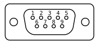
|
| Pin
|
Description
|
| 1
|
XUART4 RS485+
|
| 2
|
Debug Console RS232 RXD
|
| 3
|
Debug Console RS232 TXD
|
| 4
|
Not Connected
|
| 5
|
Ground
|
| 6
|
XUART4 RS485-
|
| 7
|
XUART2 RS232 TXD
|
| 8
|
XUART2 RS232 RXD
|
| 9
|
Not Connected
|
|
TS-8820 Register Map
This register map assumes a base address offset. The offset when using the TS-4720 is 0x80008000. This address must first be activated using the MUXBUS enable and timing registers on the CPU module. On the TS-4720, write 0xF3FF to the address 0x80004004. Sample code for accessing the functions described in this table are largely encompassed by the ts8820ctl software available on the TS FTP Site.
| Offset
|
Bits
|
Description
|
| 0x0
|
15:0
|
Model ID: Reads 0x8820
|
| 0x2
|
15:11
|
Reserved
|
| 10
|
Pull-up 5-8 enable
|
| 9
|
Pull-up 3-4 enable
|
| 8
|
Pull-up 1-2 enable
|
| 7
|
H-bridge 2 enable (contacts go high-Z otherwise)
|
| 6
|
H-bridge 1 enable (contacts go high-Z otherwise)
|
| 5
|
H-bridge 2 direction
|
| 4
|
H-bridge 1 direction
|
| 3:0
|
FPGA Revision
|
| 0x4
|
15:14
|
Reserved
|
| 13:0
|
Digital inputs 14:1
|
| 0x6
|
15:10
|
Reserved
|
| 9:0
|
SRAM Page register
|
| 0x8
|
15:12
|
Reserved
|
| 11:6
|
Override Digital Outputs 6:1 with PWM
|
| 5:0
|
Digital Output Values 6:1
|
| 0xa
|
15:0
|
Reserved
|
| 0xc
|
15:0
|
Reserved
|
| 0xe
|
15:0
|
Reserved
|
| 0x10
|
15:13
|
PWM #1 Prescaler
|
| 12:0
|
PWM #1 Duty Cycle
|
| 0x12
|
15:13
|
PWM #2 Prescalar
|
| 12:0
|
PWM #2 Duty Cycle
|
| 0x14
|
15:13
|
PWM #3 Prescaler
|
| 12:0
|
PWM #3 Duty Cycle
|
| 0x16
|
15:13
|
PWM #4 Prescaler
|
| 12:0
|
PWM #4 Duty Cycle
|
| 0x18
|
15:13
|
PWM #5 Prescaler
|
| 12:0
|
PWM #5 Duty Cycle
|
| 0x1a
|
15:13
|
PWM #6 Prescaler
|
| 12:0
|
PWM #6 Duty Cycle
|
| 0x1c
|
15:13
|
PWM #7 Prescaler
|
| 12:0
|
PWM #7 Duty Cycle
|
| 0x1e
|
15:13
|
PWM #8 Prescaler
|
| 12:0
|
PWM #8 Duty Cycle
|
| 0x20
|
15:0
|
Pulse Counter #1 (RO)
|
| 0x22
|
15:0
|
Pulse Counter #2 (RO)
|
| 0x24
|
15:0
|
Pulse Counter #3 (RO)
|
| 0x26
|
15:0
|
Pulse Counter #4 (RO)
|
| 0x28
|
15:0
|
Pulse Counter #5 (RO)
|
| 0x2a
|
15:0
|
Pulse Counter #6 (RO)
|
| 0x2c
|
15:0
|
Pulse Counter #7 (RO)
|
| 0x2e
|
15:0
|
Pulse Counter #8 (RO)
|
| 0x30
|
15:0
|
Pulse Counter #9 (RO)
|
| 0x32
|
15:0
|
Pulse Counter #10 (RO)
|
| 0x34
|
15:0
|
Pulse Counter #11 (RO)
|
| 0x36
|
15:0
|
Pulse Counter #12 (RO)
|
| 0x38
|
15:0
|
Pulse Counter #13 (RO)
|
| 0x3a
|
15:0
|
Pulse Counter #14 (RO)
|
| 0x3c
|
15:0
|
Reserved
|
| 0x3e
|
15:0
|
Reserved
|
| 0x80
|
15:0
|
ADC Core ID (reads 0xadc1)
|
| 0x82
|
15:8
|
ADC Channel Mask (0 = do not save channel data)
|
| 7:6
|
Highest number chip to use (0-3, if 01 then sample chip 0 and chip 1)
|
| 5
|
1 = Force standby
|
| 4
|
1 = Use standby between samples to save power
|
| 3
|
1 = Smart DMA IRQ mode
|
| 2
|
1 = Enable IRQ
|
| 1
|
1 = Collect samples, 0 = stop
|
| 0
|
1 = Reset ADC chips and all FIFOs
|
| 0x84
|
15
|
1 = There has been a FIFO overflow since last reset
|
| 14:0
|
Number of samples available to be read
|
| 0x86
|
15:0
|
Sample Data (RO)
|
| 0x88
|
15:0
|
Sampling period LSB (RW)
|
| 0x8a
|
15:0
|
Sampling period MSB (RW)
|
| 0x8c
|
15:0
|
IRQ Threshold (RW)
|
| 0x8e
|
15:0
|
DMA transfer size for smart mode (RW) (TODO)
|
| 0x90
|
15:0
|
Reserved
|
| 0x92
|
15:0
|
Reserved
|
| 0x94
|
15:0
|
Reserved
|
| 0x96
|
15:0
|
Reserved
|
| 0x98
|
15:0
|
Reserved
|
| 0x9a
|
15:0
|
Reserved
|
| 0x9c
|
15:0
|
Reserved
|
| 0x9e
|
15:0
|
Reserved
|
| 0xa0
|
15:0
|
DAC 1 Control Register
|
| 0xa2
|
15:0
|
DAC 2 Control Register
|
| 0xa4
|
15:0
|
DAC 3 Control Register
|
| 0xa6
|
15:0
|
DAC 4 Control Register
|
Product Notes
FCC Advisory
This equipment generates, uses, and can radiate radio frequency energy and if not installed and used properly (that is, in strict accordance with the manufacturer's instructions), may cause interference to radio and television reception. It has been type tested and found to comply with the limits for a Class A digital device in accordance with the specifications in Part 15 of FCC Rules, which are designed to provide reasonable protection against such interference when operated in a commercial environment. Operation of this equipment in a residential area is likely to cause interference, in which case the owner will be required to correct the interference at his own expense.
If this equipment does cause interference, which can be determined by turning the unit on and off, the user is encouraged to try the following measures to correct the interference:
Reorient the receiving antenna.
Relocate the unit with respect to the receiver.
Plug the unit into a different outlet so that the unit and receiver are on different branch circuits.
Ensure that mounting screws and connector attachment screws are tightly secured.
Ensure that good quality, shielded, and grounded cables are used for all data communications.
If necessary, the user should consult the dealer or an experienced radio/television technician for additional suggestions.
The following booklets prepared by the Federal Communications Commission (FCC) may also prove helpful:
How to Identify and Resolve Radio-TV Interference Problems (Stock No. 004-000-000345-4)
Interface Handbook (Stock No. 004-000-004505-7)
These booklets may be purchased from the Superintendent of Documents, U.S. Government Printing Office, Washington, DC 20402.
Limited Warranty
See our Terms and Conditions for more details.


