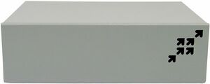
TS-ENC730
 | |
| Documents | |
|---|---|
| Schematic |
Overview
The TS-ENC730 metal enclosure is made to house the TS-7300 Single Board Computer and up to two PC/104 peripheral boards. The internal power regulator efficiently converts unregulated 7-28 VDC input into regulated +5 VDC as required by the SBC. Sleep mode allows current drain of 200 microAmps with programmable sleep periods. The TS-ENC730 also brings out some features implemented on the TS-7300 FPGA, such as the SJA1000 CAN core, PWM for the DAC lines, 800x600 VGA Video, second ethernet port, additional serial ports, etc. In addition, the TS-ENC730 includes the TS-732 daughter board for the TS-7300 onboard FPGA. The AVR microcontroller on the TS-732 implements ADC/GPIO/LEDs extra functionalities. Also, the physical layer for the CAN bus is provided by the TS-732.
Features
The TS-ENC730 Rugged Enclosure provides extra functions, including power converter, AVR microcontroller daughter board and CAN Phy. Additional features include:
- 8-28 VDC power input
- User programmable low power sleep mode (300 uA)
- Surge suppression on power input
- Terminal strip with 8 I/O
- 4 channel 10 bit ADC 0V - 5V (12-16 bits effective*)
- 2 channel 12 bit high power DAC 0V - 10V (sync/source 300mA)
- 4 high current GPIO pins (sync/source 400 mA)
- 5-8 COM ports
- Two software controlled LEDs
- Status LEDs for both Ethernet ports
- Optional CAN bus port with Linux driver available
- Linux Application available for ADC/DAC/GPIO/LEDs control
- Sturdy metal design reduces noise
TS-ENC730 FPGA
The TS-ENC730 includes a TS-7300 FPGA core designed specially for the TS-ENC730 and the TS-732 daughter companion board. This FPGA core talks to the AVR Microcontroller on the TS-732 via a UART interface, making use of the 8x baud clock reference provided by the AVR. This FPGA core also implements a SJA1000 CAN controller and 2 PWM channels for the TS-732 DAC circuitry. The registers that control these functions appear in the memory space of the ARM9 processor dedicated for the FPGA functions, therefore they can be accessed through the Linux OS and programming. The base address used is 0x7200_0400 and the register are 16-bit wide.
Register Map
| I/O Address | Description | Data Bits |
|---|---|---|
| Base + 0 | Control Register | bits 3:15 – reserved
bit 2: CAN controller enable bit 1: PWM channel #1 enable bit 0: PWM channel #0 enable |
| Base + 2 | PWM channel #0 high-time | |
| Base + 4 | PWM channel #0 low-time | |
| Base + 6 | PWM channel #1 high-time | |
| Base + 8 | PWM channel #1 low-time | |
| Base + A | AVR clock reference | |
| Base + C | AVR UART STAT register | |
| Base + E | AVR UART RXDAT/TXDAT register | |
| Base + 100 | CAN controller regs start | SJA1000: 256 byte x 8bit registers |
The AVR clock reference represents the current frequency/2 of the clock coming
out the AVR. Nominally this should be 100Khz. Register value is updated twice per
second.