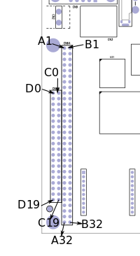
TS-7250-V3 PC104 Header

From embeddedTS Manuals

The PC/104 connector consists of four rows of pins labelled A-D. This header implements the #PC104 Bus, and optionally most pins can be GPIO.

Refer to the IO specifications for details on the IO voltages of these pins. Not all pins on the PC/104 bus are designed to be 5V tolerant, but will be in places where it is needed for compatibility with the bus.

Pins IO Specification
D3-D15 [1] PCA9555
A1 CPU 3.3V
A10, A11, A12-A31, B6, B8, B11-B20, B25-B28, B30, D1-D2 FPGA 3.3-V LVTTL
A2-A9, B4, B21-B23, C11-C18 FPGA 3.3-V LVTTL+QS3861
B2 Open drain with pull to 5V
  1. These are only present on the models with the optional I2C port expander

TS-7250-V3 PC104 pinout.svg

Pin Description Pin Description Pin Description Pin Description
B32 GND A32 GND
B31 GND A31 ISA_ADD_00/Chip 50004064.fpga_gpio IO 0
B30 ISA_14_3_MHZ [1] A30 ISA_ADD_01/Chip 50004064.fpga_gpio IO 1
B29 +5V [2] A29 ISA_ADD_02/Chip 50004064.fpga_gpio IO 2
B28 Chip 50004040.fpga_gpio IO 1/TS mode DAT15 A28 ISA_ADD_03/Chip 50004064.fpga_gpio IO 3 C19 GND D19 GND
B27 Chip 50004040.fpga_gpio IO 2/TS mode DAT14 A27 ISA_ADD_04/Chip 50004064.fpga_gpio IO 4 C18 ISA_DAT_15/Chip 5000405c.fpga_gpio IO 15 D18 GND
B26 Chip 50004040.fpga_gpio IO 10/TS mode DAT13 A26 ISA_ADD_05/Chip 50004064.fpga_gpio IO 5 C17 ISA_DAT_14/Chip 5000405c.fpga_gpio IO 14 D17 Unused
B25 FPGA IRQ 13/TS mode DAT11 A25 ISA_ADD_06/Chip 50004064.fpga_gpio IO 6 C16 ISA_DAT_13/Chip 5000405c.fpga_gpio IO 13 D16 +5V [2]
B24 GND A24 ISA_ADD_07/Chip 50004064.fpga_gpio IO 7 C15 ISA_DAT_12/Chip 5000405c.fpga_gpio IO 12 D15 Chip 50004054.fpga_gpio IO 12
B23 FPGA IRQ 14 A23 ISA_ADD_08/Chip 50004064.fpga_gpio IO 8 C14 ISA_DAT_11/Chip 5000405c.fpga_gpio IO 11 D14 Chip 50004054.fpga_gpio IO 11
B22 FPGA IRQ 15 A22 ISA_ADD_09/Chip 50004064.fpga_gpio IO 9 C13 ISA_DAT_10/Chip 5000405c.fpga_gpio IO 10 D13 Chip 50004054.fpga_gpio IO 10
B21 FPGA IRQ 16 A21 ISA_ADD_10/Chip 50004064.fpga_gpio IO 10 C12 ISA_DAT_09/Chip 5000405c.fpga_gpio IO 9 D12 Chip 50004054.fpga_gpio IO 9
B20 TS mode DAT12 A20 ISA_ADD_11/Chip 50004064.fpga_gpio IO 11 C11 ISA_DAT_08/Chip 5000405c.fpga_gpio IO 8 D11 Chip 50004054.fpga_gpio IO 8
B19 Chip 50004040.fpga_gpio IO 6 A19 ISA_ADD_12/Chip 50004064.fpga_gpio IO 12 C10 Unused D10 Chip 50004054.fpga_gpio IO 7
B18 Chip 50004040.fpga_gpio IO 7/TS mode DAT10 A18 ISA_ADD_13/Chip 50004064.fpga_gpio IO 13 C09 Unused D09 Chip 50004054.fpga_gpio IO 6
B17 Chip 50004040.fpga_gpio IO 8/TS mode DAT9 A17 ISA_ADD_14/Chip 50004064.fpga_gpio IO 14 C08 Unused D08 Chip 50004054.fpga_gpio IO 5
B16 Chip 50004040.fpga_gpio IO 12 A16 ISA_ADD_15/Chip 50004064.fpga_gpio IO 15 C07 Unused D07 Chip 50004054.fpga_gpio IO 4
B15 Chip 50004040.fpga_gpio IO 13 A15 ISA_ADD_16/Chip 5000406c.fpga_gpio IO 0 C06 Unused D06 Chip 50004054.fpga_gpio IO 3
B14 ISA_IOR/Chip 5000406c.fpga_gpio IO 4 A14 ISA_ADD_17/Chip 5000406c.fpga_gpio IO 1 C05 Unused D05 Chip 50004054.fpga_gpio IO 2
B13 ISA_IOW/Chip 5000406c.fpga_gpio IO 5 A13 ISA_ADD_18/Chip 5000406c.fpga_gpio IO 2 C04 Unused D04 Chip 50004054.fpga_gpio IO 1
B12 ISA_MEMR/Chip 5000406c.fpga_gpio IO 6 A12 ISA_ADD_19/Chip 5000406c.fpga_gpio IO 3 C03 Unused D03 Chip 50004054.fpga_gpio IO 0
B11 ISA_MEMW/Chip 5000406c.fpga_gpio IO 7 A11 ISA_AEN/Chip 50004040.fpga_gpio IO 0 C02 Unused D02 Chip 5000406c.fpga_gpio IO 9
B10 GND A10 Chip 50004040.fpga_gpio IO 5 C01 Unused D01 Chip 5000406c.fpga_gpio IO 8
B09 8V_48V [3] A09 ISA_DAT_00/Chip 5000405c.fpga_gpio IO 0 C00 GND D00 GND
B08 Chip 50004040.fpga_gpio IO 3 A08 ISA_DAT_01/Chip 5000405c.fpga_gpio IO 1
B07 Unused A07 ISA_DAT_03/Chip 5000405c.fpga_gpio IO 3
B06 Chip 50004040.fpga_gpio IO 9 A06 ISA_DAT_04/Chip 5000405c.fpga_gpio IO 4
B05 N/A A05 ISA_DAT_05/Chip 5000405c.fpga_gpio IO 5
B04 FPGA IRQ 17/TS mode DAT8 A04 ISA_DAT_02/Chip 5000405c.fpga_gpio IO 2
B03 +5V [2] A03 ISA_DAT_06/Chip 5000405c.fpga_gpio IO 6
B02 Chip 20a4000.gpio IO 7 [4] A02 ISA_DAT_07/Chip 5000405c.fpga_gpio IO 7
B01 GND A01 Chip 20a4000.gpio IO 8
  1. Outputs a continuous 14.318180 MHz clock
  2. 2.0 2.1 2.2 Powering the system from PC104 5V prevents the Board's low power sleep mode from functioning.
  3. This pin can be used to supply power to the board through the switching regulator.
  4. This is automatically pulsed on startup by the ts-pc104 driver as ISA_RESET