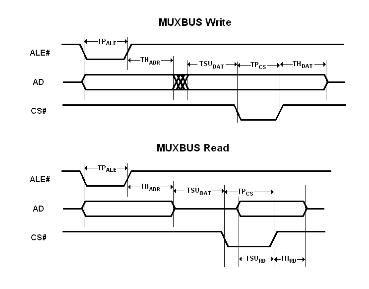
Generic MUXBUS

All TS-SOCKET System-on-Modules have an external bus called the MUXBUS. The bus consists of 16 muxed address/data lines, ALE#, CS#, DIR, BHE#, and WAIT#. The MUXBUS provides a way for TS-SOCKET base board designers to include static memory devices, bridges to other industry standard buses such as PC/104, or an FPGA that implements custom features. Verilog modules ts8100.v and muxbusbridge.v are provided as examples of how to interface with the MUXBUS.
MUXBUS slaves can be 8 bit or 16 bit devices. Each SoM has an 8 bit MUXBUS address space which must be accessed with 8 bit reads and writes, and a 16 bit MUXBUS address space which must be accessed with 16 bit reads and writes. Software that works with the MUXBUS must know whether it is talking to an 8 bit or 16 bit slave device and act accordingly.
The bus cycle speed depends on the FPGA clock speed, which varies from one SoM to another. Thus, the MUXBUS behavior is specified in clock cycles. The bus cycle works as follows:
- ALE# is asserted, and the address is driven on the bus lines. This condition is held for TP_ALE + 1 clock cycles.
- ALE# is de-asserted while the address remains valid for TH_ADR + 1 clock cycles.
- Data is driven on the bus lines (for a write) or the bus lines go high-Z (for a read) for TSU_DAT + 1 clock cycles.
- CS# is asserted for TP_CS + 1 clock cycles.
- CS# is de-asserted and data remains valid for TH_DAT + 1 clock cycles.
BHE# and DIR remain valid throughout the whole bus cycle. WAIT# is an input. The external device can assert the WAIT signal during the CS# pulse to extend it. The bus can work in 8 bit or 16 bit modes. In 8 bit mode, mux lines 8-15 are not used for data and BHE# is ignored. In 16 bit mode, byte reads and writes are still supported using BHE# and A0.
Each module will have a 16 bit external bus configuration register in its #Syscon.
| Bus Config Register Bits | Usage |
|---|---|
| bit 0 | Bus enable (otherwise, pins are GPIO or reserved) |
| bits 2:1 | TP_ALE |
| bits 4:3 | TH_ADR |
| bits 6:5 | TSU_DAT |
| bits 12:7 | TP_CS [1] |
| bits 15:13 | TH_DAT |
- ↑ A TP_CS of 0x3f is not supported -- use a value from 0 to 62 (that's 0x00 to 0x3e).
IMPLEMENTATION TIMING NOTES:
On a MUXBUS write, all timing values are controlled by the bus config register. The slave device is permitted to latch data on either the leading edge or the trailing edge of the CS# pulse, or any time in between.
One a MUXBUS read, the MUXBUS latches data on the trailing edge of the CS# pulse. The slave device should begin driving the data bus in response to CS# assertion. Users should program TP_CS so that TSU_RD is at least 10ns plus any delays between the two boards. A conservative TP_CS setting is recommended, because an extra clock cycle here will not have a significant effect on net MUXBUS bandwidth.
The slave device must stop driving the data bus in response to CS# de-assertion. TH_RD must be at most 30ns.