TS-4900 TS-Socket interface

From embeddedTS Manuals

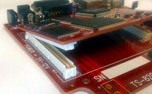
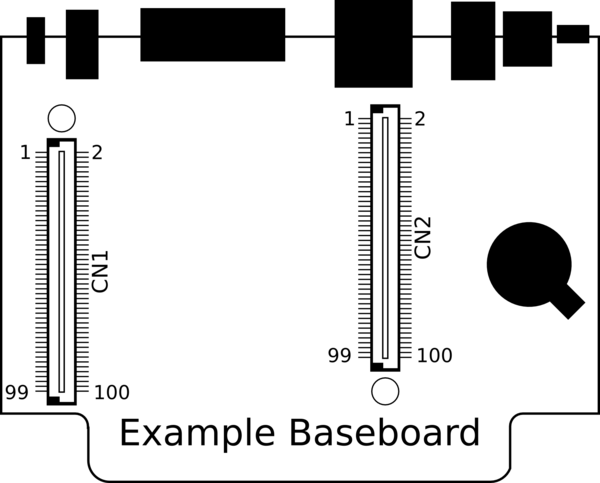
The TS-SOCKET System-on-Modules (SoMs) all use two high density 100 pin connectors for power and all I/O. These follow a common pinout for various external interfaces so new modules can be dropped in to lower power consumption or use a more powerful processor. The male connector is on the baseboard, and the female connector is on the SoM. You can find the datasheet for the baseboard's male connector here. This can be ordered from the TS-Socket SoM product page as CN-TSSOCKET-M-10 for a 10 pack, or CN-TSSOCKET-M-100 for 100 pieces.

TS-Socket

In our schematics and our table layout below, we refer to pin 1 from the male connector on the baseboard. For designing a custom carrier board for the TS-4900 we recommend using the TS-8550 as a base: https://www.embeddedTS.com/documentation/ts-8550-schematic.pdf

Pin Name IO Type
CN1_001 NC N/A
CN1_002 EXT_RESET# [1] Open Drain Input 3.3V
CN1_003 NC N/A
CN1_004 EN_USB_5V [2] Single Ended 3.3V
CN1_005 NC N/A
CN1_006 SD2_D2 [3] Single Ended 3.3V
CN1_007 NC N/A
CN1_008 SD2_D3 [3] Single Ended 3.3V
CN1_009 OFF_BD_RESET# [4] Single Ended 3.3V
CN1_010 SD2_CMD [3] Single Ended 3.3V
CN1_011 NC N/A
CN1_012 3.3V 3.3V
CN1_013 NC Single Ended 3.3V
CN1_014 SD2_CLK [3] Single Ended 3.3V
CN1_015 5V [5] Single Ended 3.3V
CN1_016 5V [5] Single Ended 3.3V
CN1_017 NC Single Ended 3.3V
CN1_018 SD2_D0 [3] Single Ended 3.3V
CN1_019 LCD_D08 Single Ended 3.3V
CN1_020 SD2_D1 [3] Single Ended 3.3V
CN1_021 LCD_D09 Single Ended 3.3V
CN1_022 NC Single Ended 3.3V
CN1_023 LCD_D10 Single Ended 3.3V
CN1_024 LCD_D00 Single Ended 3.3V
CN1_025 LCD_D11 Single Ended 3.3V
CN1_026 LCD_D01 Single Ended 3.3V
CN1_027 LCD_D12 Single Ended 3.3V
CN1_028 LCD_D02 Single Ended 3.3V
CN1_029 5V [5] Single Ended 3.3V
CN1_030 LCD_D03 Single Ended 3.3V
CN1_031 LCD_D13 Single Ended 3.3V
CN1_032 LCD_D04 Single Ended 3.3V
CN1_033 LCD_D14 Single Ended 3.3V
CN1_034 LCD_D05 Single Ended 3.3V
CN1_035 LCD_D15 Single Ended 3.3V
CN1_036 V_BAT Single Ended 3.3V
CN1_037 LCD_D16 Single Ended 3.3V
CN1_038 LCD_D06 Single Ended 3.3V
CN1_039 LCD_D17 Single Ended 3.3V
CN1_040 LCD_D07 Single Ended 3.3V
CN1_041 LCD_D18 Single Ended 3.3V
CN1_042 LCD_D21 Single Ended 3.3V
CN1_043 LCD_D19 Single Ended 3.3V
CN1_044 LCD_D22 Single Ended 3.3V
CN1_045 LCD_D20 Single Ended 3.3V
CN1_046 LCD_D23 Single Ended 3.3V
CN1_047 5V [5] Single Ended 3.3V
CN1_048 EN_LCD_3.3V Single Ended 3.3V
CN1_049 LCD_CLK Single Ended 3.3V
CN1_050 NC Single Ended 3.3V
CN1_051 LCD_HSYNC Single Ended 3.3V
CN1_052 BOOT_MODE_0 Single Ended 3.3V
CN1_053 LCD_VSYNC Single Ended 3.3V
CN1_054 BOOT_MODE_1 Single Ended 3.3V
CN1_055 LCD_DE Single Ended 3.3V
CN1_056 SPI_1_MISO Single Ended 3.3V
CN1_057 LCD_PWM Single Ended 3.3V
CN1_058 SPI_1_MOSI Single Ended 3.3V
CN1_059 SPI_FLASH_CS# [6] Single Ended 3.3V
CN1_060 SPI_1_CLK Single Ended 3.3V
CN1_061 SPI_1_CS1# Single Ended 3.3V
CN1_062 Ground Single Ended 3.3V
CN1_063 CN1-63 / ttymxc3 TXEN Single Ended 3.3V
CN1_064 EIM_DA15 / MUX_AD_15 Single Ended 3.3V
CN1_065 EIM_EB1 Single Ended 3.3V
CN1_066 EIM_DA14 / MUX_AD_14 Single Ended 3.3V
CN1_067 CN1-67 / ttymxc1 TXEN Single Ended 3.3V
CN1_068 EIM_DA13 / MUX_AD_13 Single Ended 3.3V
CN1_069 CAN2_RXD Single Ended 3.3V
CN1_070 EIM_DA12 / MUX_AD_12 Single Ended 3.3V
CN1_071 CAN2_TXD Single Ended 3.3V
CN1_072 EIM_DA11 / MUX_AD_11 Single Ended 3.3V
CN1_073 PUSH_SW# Single Ended 3.3V
CN1_074 EIM_DA10 / MUX_AD_10 Single Ended 3.3V
CN1_075 Ground Single Ended 3.3V
CN1_076 EIM_DA09 / MUX_AD_09 Single Ended 3.3V
CN1_077 EIM_A21 Single Ended 3.3V
CN1_078 EIM_DA08 / MUX_AD_08 Single Ended 3.3V
CN1_079 EIM_BCLK Single Ended 3.3V
CN1_080 EIM_DA07 / MUX_AD_07 Single Ended 3.3V
CN1_081 EIM_A18 Single Ended 3.3V
CN1_082 EIM_DA06 / MUX_AD_06 Single Ended 3.3V
CN1_083 EIM_OE Single Ended 3.3V
CN1_084 EIM_DA05 / MUX_AD_05 Single Ended 3.3V
CN1_085 EIM_A20 Single Ended 3.3V
CN1_086 EIM_DA04 / MUX_AD_04 Single Ended 3.3V
CN1_087 CN1-87 / #Offboard Clock Single Ended 3.3V
CN1_088 EIM_DA03 / MUX_AD_03 Single Ended 3.3V
CN1_089 EIM_A22 / Offboard IRQ 69 Single Ended 3.3V
CN1_090 EIM_DA02 / MUX_AD_02 Single Ended 3.3V
CN1_091 EIM_A23 Single Ended 3.3V
CN1_092 EIM_DA03 / MUX_AD_01 Single Ended 3.3V
CN1_093 EIM_A24 Single Ended 3.3V
CN1_094 EIM_DA00 / MUX_AD_00 Single Ended 3.3V
CN1_095 Ground Single Ended 3.3V
CN1_096 EIM_LBA / BUS_ALE# Single Ended 3.3V
CN1_097 EIM_WAIT / BUS_WAIT# Single Ended 3.3V
CN1_098 EIM_RW / SDBOOT / BUS_DIR Single Ended 3.3V
CN1_099 EIM_EB1 / BUS_BHE# Single Ended 3.3V
CN1_100 EIM_CS0 /BUS_CS# Single Ended 3.3V
CN2_001 MDI_0_P Single Ended 3.3V
CN2_002 ETH_ACT_LED Single Ended 3.3V
CN2_003 MDI_0_M Single Ended 3.3V
CN2_004 ETH_LINK_LED Single Ended 3.3V
CN2_005 ETH_CT Single Ended 3.3V
CN2_006 RED_LED# Single Ended 3.3V
CN2_007 MDI_1_P Single Ended 3.3V
CN2_008 GREEN_LED# Single Ended 3.3V
CN2_009 MDI_1_M Single Ended 3.3V
CN2_010 LVDS_TX3_P Single Ended 3.3V
CN2_011 ETH_CT Single Ended 3.3V
CN2_012 LVDS_TX3_M Single Ended 3.3V
CN2_013 3.3V [7] Single Ended 3.3V
CN2_014 Ground Single Ended 3.3V
CN2_015 Ground Single Ended 3.3V
CN2_016 LVDS_TX2_P Single Ended 3.3V
CN2_017 MDI_2_P Single Ended 3.3V
CN2_018 LVDS_TX2_M Single Ended 3.3V
CN2_019 MDI_2_M Single Ended 3.3V
CN2_020 NC Single Ended 3.3V
CN2_021 Ground Single Ended 3.3V
CN2_022 LVDS_TX0_P Single Ended 3.3V
CN2_023 MDI_3_P Single Ended 3.3V
CN2_024 LVDS_TX0_M Single Ended 3.3V
CN2_025 MDI_3_M Single Ended 3.3V
CN2_026 Ground Single Ended 3.3V
CN2_027 1.2V Single Ended 3.3V
CN2_028 I2C_2_CLK Single Ended 3.3V
CN2_029 HOST_USB_M Single Ended 3.3V
CN2_030 I2C_2_DAT Single Ended 3.3V
CN2_031 HOST_USB_P Single Ended 3.3V
CN2_032 NC Single Ended 3.3V
CN2_033 1.2V Single Ended 3.3V
CN2_034 NC Single Ended 3.3V
CN2_035 USB_OTG_M Single Ended 3.3V
CN2_036 AUD_CLK Single Ended 3.3V
CN2_037 USB_OTG_P Single Ended 3.3V
CN2_038 AUD_FRM Single Ended 3.3V
CN2_039 3.3V [7] Single Ended 3.3V
CN2_040 AUD_TXD Single Ended 3.3V
CN2_041 LVDS_CLK_M Single Ended 3.3V
CN2_042 AUD_RXD Single Ended 3.3V
CN2_043 LVDS_CLK_P Single Ended 3.3V
CN2_044 Ground Single Ended 3.3V
CN2_045 Ground Single Ended 3.3V
CN2_046 LVDS_TX1_M Single Ended 3.3V
CN2_047 PCIE_TX_P Single Ended 3.3V
CN2_048 LVDS_TX1_P Single Ended 3.3V
CN2_049 PCIE_TX_M Single Ended 3.3V
CN2_050 Ground Single Ended 3.3V
CN2_051 Ground Single Ended 3.3V
CN2_052 CSI0_DAT12 Single Ended 3.3V
CN2_053 PCIE_RX_M Single Ended 3.3V
CN2_054 AUD_MCLK Single Ended 3.3V
CN2_055 PCIE_RX_P Single Ended 3.3V
CN2_056 CSI0_DAT17 Single Ended 3.3V
CN2_057 DDR_1.5V [8] Single Ended 3.3V
CN2_058 SD4_DAT7 Single Ended 3.3V
CN2_059 PCIE_CLK_P Single Ended 3.3V
CN2_060 SD3_RST Single Ended 3.3V
CN2_061 PCIE_CLK_M Single Ended 3.3V
CN2_062 GPIO_16 Single Ended 3.3V
CN2_063 1.8V [9] Single Ended 3.3V
CN2_064 GPIO_17 Single Ended 3.3V
CN2_065 SPI_2_CS# Single Ended 3.3V
CN2_066 CSI0_DAT13 Single Ended 3.3V
CN2_067 SPI_2_MOSI Single Ended 3.3V
CN2_068 GPIO_19 Single Ended 3.3V
CN2_069 SPI_2_MISO Single Ended 3.3V
CN2_070 CSI0_MCLK Single Ended 3.3V
CN2_071 SPI_2_CLK Single Ended 3.3V
CN2_072 GPIO_17 Single Ended 3.3V
CN2_073 Ground Single Ended 3.3V
CN2_074 USB_OTG_ID Single Ended 3.3V
CN2_075 SATA_RX_M Single Ended 3.3V
CN2_076 USB_OTG_VBUS Single Ended 3.3V
CN2_077 SATA_RX_P Single Ended 3.3V
CN2_078 CN2-78 / COM1 txd Single Ended 3.3V
CN2_079 3.3V Single Ended 3.3V
CN2_080 CN2-80 / COM1 rxd Single Ended 3.3V
CN2_081 SATA_TX_M Single Ended 3.3V
CN2_082 CN2-82 / COM2 txd Single Ended 3.3V
CN2_083 SATA_TX_P Single Ended 3.3V
CN2_084 CN2-84 / COM2 rxd Single Ended 3.3V
CN2_085 Ground Single Ended 3.3V
CN2_086 CN2-86 / COM3 txd Single Ended 3.3V
CN2_087 NC Single Ended 3.3V
CN2_088 CN2-88 / COM3 rxd Single Ended 3.3V
CN2_089 NC Single Ended 3.3V
CN2_090 CN2-90 / COM4 txd Single Ended 3.3V
CN2_091 NC Single Ended 3.3V
CN2_092 CN2-92 / COM4 rxd Single Ended 3.3V
CN2_093 DEBUG_TXD Single Ended 3.3V
CN2_094 CN2-94 Single Ended 3.3V
CN2_095 DEBUG_RXD Single Ended 3.3V
CN2_096 CN2-96 Single Ended 3.3V
CN2_097 CAN_1_TXD Single Ended 3.3V
CN2_098 CN2-98 Single Ended 3.3V
CN2_099 CAN_1_RXD Single Ended 3.3V
CN2_100 CN2-100 Single Ended 3.3V

Example Baseboard

  1. EXT_RESET# is an input used to reboot the CPU. Do not drive active high, use open drain.
  2. This is an output which can be manipulated in the #Syscon. This pin can optionally be connected to control a FET to a separate 5V rail for USB to allow software to reset USB devices.
  3. 3.0 3.1 3.2 3.3 3.4 3.5 This SD interface is the same one used by the MicroSD on the TS-4900. Only one can be used at a time.
  4. OFF_BD_RESET# is an output from the CPU that automatically sends a reset signal when the unit powers up or reboots. It can be connected to any IC on the base board that requires a reset.
  5. 5.0 5.1 5.2 5.3 The 5V power pins should each be connected to a 5V source.
  6. This is used during production to boot to an offboard SPI flash. This pin should typically be left unconnected.
  7. 7.0 7.1 The TS-4900 regulates a 3.3V rail which can source up to 700mA. Designs should target a 300mA max if they intend to use other SoMs.
  8. This pin is used as a test point to verify the RAM has a correct voltage for debugging
  9. This pin is used as a test point for debugging