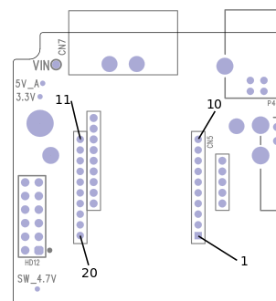
TS-7180 Nimbelink Socket
| Note: | The socket is designed to support various radios from multiple vendors. Even within the same product line, e.g. Airgain's Skywire cell modems, some modules may deviate slightly from the standards set out by the manufacturers. Due to this, we recommend reviewing the datasheet carefully for any potential modules intended to be used in combination with this platform. Our support team (email or support portal) is happy to help advise with any questions on device compatibility. |
The CN5 header is a 2mm pitch 2x10 header which supports XBEE form factor modules. These include NimbeLink and Digi cell modems, Zigbee, Digi mesh, and other third party radios.
For Cell radios that use USB this must be enabled. This turns off USB to the bottom port on the dual high type A connector. Only enable if this is compatible with your module:
# Turn on the USB
gpioset 2 12=0
This header can provide 3.3V or 4V as some cell radios require higher voltage. Check the datasheet of your module before turning on any power to this header. Most cell modems require 4V, while most other radios require 3.3V.
# Only turn on one at a time.
# For 4V modules:
gpioset 5 17=1

# For 3.3V modules:
# gpioset 5 18=1
Many NimbeLink modems require NIMBEL_PWR_ON to be toggled before they "turn on".
If one thinks of turning on the power (above) as "attaching the battery" of a cellphone, toggling NIMBEL_PWR_ON is analogous to "pressing the power button" for a second. Here's a script to do exactly that.
gpioset 2 19=1
sleep 1
gpioset 2 19=0
If your device doesn't turn on or off as expected, be sure to consult the manual for it. There are often device-specific procedures for powering on and sometimes even custom AT command sequences needed in order to safely power off.
By default there is no UART mapped to this header. Map ttymxc2 with:
tshwctl --addr 307 --poke 1 # Claim bluetooth UART3 (ttymxc2) for modem
See the #FPGA Registers address 307 for more UART options.
For serial modules refer to these related links:
- Technologic Systems: A friendly introduction to XBEE
- Digi's C library for XBEE API mode
- Digi's Python XBEE library
- Digi's C# Library
- Digi's Java Library
- libxbee3 (community XBEE library)
This sample code can be used to verify connectivity to the serial-based XBee modules:
wget https://files.embeddedTS.com/ts-arm-sbc/ts-7840-linux/samples/xbeetest.c
gcc xbeetest.c -o xbeetest

gpioset 5 18=1 # Turn on only 3.3V
tshwctl --addr 307 --poke 1 # Claim bluetooth UART3 (ttymxc2)
./xbeetest /dev/ttymxc2
This will print out the module information such as:
XBee3 Zigbee TH RELE: 100A
Build: Apr 16 2020 19:00:33
HV: 424E
Bootloader: 181 Compiler: 8030001
Stack: 6710
OK
| Signals | Pin Layout | ||||||||||||||||||||||||||||||||||||||||||
|---|---|---|---|---|---|---|---|---|---|---|---|---|---|---|---|---|---|---|---|---|---|---|---|---|---|---|---|---|---|---|---|---|---|---|---|---|---|---|---|---|---|---|---|
|
- ↑ This is a 5V tolerant TTL UART input.
- ↑ 2.0 2.1 By default, no uart is mapped here. These are remapped through fpga reg 307. For example, to remap UART3(/dev/ttymxc2) run "tshwctl --addr 308 --poke 1"
