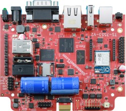
TS-7553-V2-Sandbox
| WARNING: | This is not the current latest manual for the TS-7553-V2, this is a page for testing a new layout. Please return to the TS-7553-V2 manual for the latest up to date manual! |
 | |
| Product Page | |
| Documentation | |
|---|---|
| Schematic | |
| Mechanical Drawing | |
| FTP Path | |
| Processor | |
| NXP i.MX6UL | |
| 528MHz or 696MHz Arm® Cortex®-A7 | |
| i.MX6UL Product Page |
Overview
The TS-7553-V2 is a small, embedded platform with an NXP i.MX6UL 696 MHz CPU with 512 MB DDR3 RAM. It is a spiritual successor to our TS-7553, using the same form factor and base features, but providing a more powerful CPU and many new features for overall better performance. The TS-7553-V2 can be ordered with soldered down WiFi with built in Bluetooth, our TS-SILO supercapacitor technology for safe shutdown upon power loss, non-volatile FRAM for 2 KiB of storage. There is also support for USB Gadget via the front USB Type-B socket, an internal USB host port, support for our monochrome LCD and 4 button membrane keypad, and eMMC flash for a vast improvement over the TS-7553's NAND.
Power Specifications
The TS-7553-V2 accepts a range of voltages from 5 V to 28 V DC. Note that there is a dead zone around 5.4 V, as this is the transition point from directly accepting 5 V input to changing over to the switching regulator that can accept up to 28 V. The full voltage range is accepted on the same set of power input pins.
| Input | Min voltage | Max voltage |
|---|---|---|
| 5 V input range | 4.7 | 5.3 |
| 28 V input range | 5.6 | 28 |
Power Consumption
Power consumption of the TS-7553-V2 can vary greatly depending on the build options, the peripherals in use, and the end application behavior. Most of the power savings are in the automatic CPU scaling and by disabling the Ethernet PHY. Additionally, direct 5 V input is more efficient than using a higher input voltage. This is because any input voltage above 5 V is first run through an on-board switching regulator in order to regulate it down to 5 V.
The following tests were performed on a TS-7553-V2 Rev. D PCB with the aftermarket Debian Stretch with Linux kernel 4.9 image. When the measurements were taken, the USB serial console was disconnected first to ensure the most accurate measurement possible and the TS-SILO supercapacitors were not charging during the testing. The exact model used for testing is TS-7553-V2-SMW5I. Please see Power Consumption Caveats for details on how to get these power numbers.
| Test | Input (V) | Avg. (W) | Peak (W) |
|---|---|---|---|
| CPU idle, eth0 brought down, booted from SD card, CAN disabled | 5 VDC | 0.385 W | 0.525 W |
| CPU idle, eth0 linked, booted from SD, CAN disabled | 5 VDC | 0.670 W | 0.830 W |
CPU running openssl speed, eth0 linked running iperf, booted from SD, CAN enabled
|
5 VDC | 1.105 W | 1.160 W |
| CPU idle, eth0 brought down, booted from SD card, CAN disabled | 12 VDC | 0.490 W | 0.700 W |
| CPU idle, eth0 linked, booted from SD, CAN disabled | 12 VDC | 0.830 W | 0.970 W |
CPU running openssl speed, eth0 linked running iperf, booted from SD, CAN enabled
|
12 VDC | 1.320 W | 1.355 W |
Power Consumption Caveats
In order to achieve the numbers documented above, there are some operational caveats that must be noted.
- Due to the design of the Ethernet MAC/PHY of the i.MX6UL CPU and the software patterns of U-Boot and the Linux kernel, the PHY is booted to Linux in a high power state. This occurs even though Linux leaves the interface unconfigured and down. This is because U-Boot brings up the MAC and PHY devices to configure them, but leaves them on. Lower power can be achieved by bringing the interface up and then back down if the interface is not in use; the kernel puts the PHY in a low-power state when the interface is brought down. This can be done with:
ifconfig eth0 up
ifconfig eth0 down
- The WILC WiFi device achieves the lowest power if either the kernel module (
wilc_spi) is not loaded, or if thewlan0interface is brought up but left unconfigured. If WiFi/BLE is not needed for an application, it is best to prevent thewilc_spimodule from being loaded. If only BLE is needed in an application, thewlan0interface needs to be brought up first and left active regardless. If WiFi is used in an application, then the driver will automatically handle power levels during operation of the interface.
Sleep
| Note: | As soon as the sleep command is issued the unit will go to sleep. If the proper precautions are not taken, filesystem corruption can result as the sleep mode removes all power from the CPU and other peripherals on the SBC |
The device implements a very low power sleep mode using the on-board supervisory microcontroller. This allows powering off the CPU and associated peripherals entirely for a specified period of time. This mode offers extreme power savings, only requiring around 200 mW of power, with the ability to wake up after an arbitrary timeout (up to 1847297s, which is 21d 9h 8m 17s) with a 1s resolution.
Note however, that if using the TS-SILO supercapacitors, if external power is removed but the supercapacitors have enough of a charge to keep the microcontroller powered, re-applying power will not boot the device up as the microcontroller is still in sleep mode.
CPU & Integrated Serial Interfaces
Processor
This device uses the i.MX6UL CPU, running at up to 696 MHz, based upon a Cortex-A7 core and targeting low power consumption.
Refer to NXP's documentation for more detailed information on the i.MX6UL.
I2C
The i.MX6UL supports standard I2C operation at 100 kHz, or fast mode operation at 400 kHz. The TS-7553-V2 uses three CPU I2C buses for onboard devices and external expansion. Refer to the software manual (associated with the chosen software image) for additional details on how to configure and implement I2C.
The list of I2C buses below shows their logical bus numbers as well as the device number enumerated by the Linux kernel.
| I2C# | I2C Device | Address | Description |
|---|---|---|---|
| CPU I2C1 | I2c-0 | 0x2a | Supervisory microcontroller |
| 0x68 | Battery backed RTC | ||
| CPU I2C2 | I2c-2 | N/A | Daughter Card I2C header (HD1 Pin Header) |
| CPU I2C3 | I2c-3 | 0x68 | Optional MPU-9250 IMU |
- CPU I2C1 (I2c-0) —I2C 1 bus is used for onboard system management devices, including the supervisory microcontroller and the battery-backed real-time clock (RTC). This bus is used with CPU GPIO pins rather than an internal SPI peripheral.
- CPU I2C2 (I2c-2) —I2C 2 bus is routed to the HD1 daughter card header and is intended for general-purpose I2C expansion. I2C 2 may be connected to supported embeddedTS daughter cards or custom user-designed hardware. No other devices are connected to the I2C 2 bus, leaving the full I2C address range available. This bus is used with CPU GPIO pins rather than an internal SPI peripheral.
- CPU I2C3 (I2c-3) —I2C 3 bus is connected internally to the optional onboard IMU (gyroscope, accelerometer, and magnetometer). Like CPU I2C1, this bus is used with CPU GPIO pins rather than an internal SPI peripheral.
Additional I2C buses may be implemented using available GPIO pins if further interfaces are required. An example configuration is available in the software documentation.
SPI
The i.MX6UL CPU has a native SPI peripheral that is used in a number of places on the TS-7553-V2. Additionally, kernel spidev support is added to allow SPI access from userspace. User SPI can be used for LCD access, a generic SPI connection on HD1, as well as user accessible FRAM.
The ECSPI peripheral in the i.MX6UL CPU is highly flexible and can even support SPI slave mode. For more information on the peripheral itself, please see the CPU reference manual.
UARTs
The i.MX6UL CPU on the TS-7553-V2 provides eight UART interfaces. These UARTs are implemented using the CPU UART peripherals and are routed to a combination of onboard functions, external connectors, and expansion headers. Refer to the software manual for the software image in use for additional details on UART configuration, device naming, and console assignment. The table below lists the available UARTs, their Linux device names, electrical interface type, and the physical locations of their signals.
| CPU UART # | UART Dev Name | Type | TX / + Location | RX / - Location | RTS Location | CTS Location |
|---|---|---|---|---|---|---|
| 0 | ttymxc0 | USB Console | N/A | N/A | N/A | N/A |
| 1 | ttymxc1 | RS-485 | CN9_1 / P1_3 / HD2_1 | CN9_6 / P1_4 / HD2_6 | N/A | N/A |
| 2 | ttymxc2 | Bluetooth | N/A | N/A | N/A | N/A |
| 3 | ttymxc3 | RS-232[1] | HD2_3 | HD2_2 | N/A | N/A |
| 4 | ttymxc4 | RS-232[1] | HD2_7 | HD2_8 | N/A | N/A |
| 5 | ttymxc5 | RS-232[1] | CN9_3 | CN9_2 | CN9_7[2][3] | CN9_8[2][4] |
| 6 | ttymxc6 | TTL | HD1_12 | HD1_10[5] | N/A | N/A |
| 7 | ttymxc7 | XBee/TTL | CN5_3 | CN5_2 | N/A | N/A |
RS-485
The TS-7553-V2 has a single RS-485 port that supports automatic TXEN via kernel driver features and a GPIO pin.
Memory & Storage Interfaces
eMMC Interface
The TS-7553-V2 includes a soldered down eMMC IC to provide on-board flash media. i.MX6UL SD card controller supports the MMC specification. Our off-the-shelf builds are 4 GB, but up to 64 GB are available for customized builds.
The eMMC module has a similar concern by default to SD cards in that they should not be powered down during a write/erase cycle. However, this eMMC module includes support for setting a fuse for a "Write Reliability" mode, and a "psuedo SLC (pSLC)" mode. With both enabled, all writes will be atomic to 512 B and each NAND cell will be treated as a single layer rather than a multi-layer cell. If a sector is being written during a power loss, a block is guaranteed to have either the old or new data. Even in cases where the wrong data is present on the next boot, fsck is often able to deal with the older data being present in a 512 B block.
The downside to setting these modes are that it will reduce the overall write speed and halve the available space on the eMMC to roughly 1.759 GB. Please note that even with these settings, embeddedTS strongly recommends designing the end application to eliminate any situations where a power-loss event can occur while any disk is mounted as read/write. The TS-SILO option for the TS-7553-V2 can help to eliminate the dangerous situation.
| WARNING: | Enabling these modes causes all data on the disk to become invalid and must be rewritten. Do not attempt to run the 'mmc' commands from the script individually, as all steps in the script must occur as they are or the unit may be unable to boot. If there are any failures of the script, care must be taken to resolve any issues while the unit is still booted or it may fail to boot in the future. |
| WARNING: | The script is only compatible with Rev. D or newer PCBs. Running the script on any previous PCB revision WILL result in the unit being unable to boot! There is no safe way to enable these modes on previous PCB revisions. |
| Note: | Enabling these modes is a one-way operation, it is not possible to undo them once they are made. Because of this, setting these eMMC modes will invalidate Technologic Systems' return/replacement warranty on the unit. See the warranty section for more information on this. |
FRAM
This platform supports a soldered-down, non-volatile Ferroelectric RAM (FRAM) device. The Cypress FM25L16B is a 2 KiB FRAM device in a configuration not unlike an SPI EEPROM. The nature of FRAM means it is non-volatile, incredibly fast to write, and is specified with 100 trillion read/write cycles (per each of the 256 sequential 8 byte rows) with a 150 year data retention at temperatures below 65 °C. The device is connected to Linux and presents itself as a flat file that can be read and written like any standard Linux file.
microSD Card Interface
The i.MX6UL SD card controller internal to the CPU provides support for microSD cards and is fully compliant with the SD specification. This controller has been tested with Sandisk Extreme SD cards which allow Read speeds up to 20.5MB/s and Write speeds up to 21.5MB/s.
Communications
USB
The TS-7553-V2 offers multiple USB 2.0 host ports as well as OTG (On-The-Go) compatible ports. An onboard USB hub fans out the CPU USB host interface to multiple places, allowing simultaneous use of several USB devices.
Refer to the software manual for the software image in use for additional details on USB configuration, OTG mode selection, and gadget support. Additional details are also provided in the DIO section of this manual.
USB Host Ports
The TS-7553-V2 includes two USB 2.0 host ports provided through an onboard USB hub. There is a single external USB Type-A port, and a single internal USB Type-A port. The internal port is provided by a USB Type-A connector that is mechanically oriented so that the USB dongles can fit entirely within the TS-7553-V2 enclosure.
USB Device / OTG Port
The TS-7553-V2 has a single exposed USB Type-B female port capable of USB device or OTG operation. By default, this USB device connector is routed to the supervisory microcontroller and presents a USB serial interface to the host system. However, it is possible to re-route the connector to the CPU USB OTG interface to enable USB gadget. Configuration requirements and usage details depend on the software image in use and are described in the software manual.
| USB INTERFACE | MODE | CONNECTOR | DESCRIPTION |
|---|---|---|---|
| USB HOST(via hub) | HOST | External USB Type-A | External USB host port for peripherals |
| USB HOST (via hub) | HOST | Internal USB Type-A | Internal USB host port intended for USB dongles; connector orientation allows devices to lay flat within the enclosure |
| USB OTG / Device | Device / OTG | USB Type-B (female) | Exposed USB device port; defaults to supervisory microcontroller USB serial interface |
USB Gadget
The USB Type-B female connector by default provides a USB serial console via the supervisory microcontroller. The TS-7553-V2 provides an internal USB mux IC that can be switched to connect the CPU USB OTG port to the USB Type-B female connector.
CAN
| Note: | The TS-7553-V2 Rev. B PCB does not have software control of the CAN_EN# pin for the transceivers and they are always enabled. This is addressed in later hardware revisions. |
The i.MX6UL CPU has two FlexCAN ports which are available on the DB-9 Header and the HD2 COM 2 Header The CAN interfaces support CAN 2.0B and are compatible with ISO 11898 physical layer standards. Bitrates up to 1 Mbit/s are supported, subject to bus topology and transceiver limitations.
| CAN# | CAN CONTROLLER | CAN_H LOCATION | CAN_L LOCATION | TERMINATION | NOTES |
|---|---|---|---|---|---|
| CPU Flexcan1 | FlexCAN | DB9 HEADER_PIN_4 | DB9 HEADER_PIN_9 | None | Transceiver always enabled on REV. b |
| CPU Flexcan2 | FlexCAN | HD2 COM2 HEADER_PIN_4 | HD2 COM2 HEADER_PIN_9 | None | Transceiver always enabled on REV. b |
Ethernet Port
The NXP processor implements a 10/100 ethernet controller with support built into the Linux kernel. Standard Linux utilities such as ifconfig/ip can be used to control this interface. See the Configuring the Network section for more details. For the specifics of this interface see the CPU manual.
FEC PTP Support
The i.MX6UL CPU Ethernet supports 1588 PTP (PTPv1 & PTPv2).
PTP is supported in Linux via the linuxptp project. This allows synchronizing the system clock to within ±1 us.
Wi-Fi
This board uses an ATWILC3000-MR110CA IEEE 802.11 b/g/n Link Controller Module With Integrated Bluetooth® 4.0. Linux provides support for this module using the wilc3000 driver.
Summary features:
- IEEE 802.11 b/g/n RF/PHY/MAC SOC
- IEEE 802.11 b/g/n (1x1) for up to 72 Mbps PHY rate
- Single spatial stream in 2.4GHz ISM band
- Integrated PA and T/R Switch Integrated Chip Antenna
- Superior Sensitivity and Range via advanced PHY signal processing
- Advanced Equalization and Channel Estimation
- Advanced Carrier and Timing Synchronization
- Wi-Fi Direct and Soft-AP support
- Supports IEEE 802.11 WEP, WPA, and WPA2 Security
- Supports China WAPI security
- Operating temperature range of -40°C to +85°C
Bluetooth
The Wi-Fi option for this platform also includes a Bluetooth 5.0 LE module. Support for Bluetooth is provided by the BlueZ project.
Please note that the Bluetooth module requires the modem control lines CTS and RTS as flow control when running at higher baud rates. It is possible to run the module at the initial 115200 baud if the flow control lines are unwanted.
Peripherals & Interfaces
Digital I/O (DIO)
The TS-7553-V2 offers DIO and a single Relay. The DIO exposed to various headers and terminals are controlled via the CPU. All DIO are 3.3V tolerant unless otherwise noted. All DIO pins have a pullup resistor to 3.3V.
When configured as an output, a GPIO line is driven low (GND) or high (3.3 V) by setting its output value through the GPIO character device. When configured as an input, GPIO lines use internal pull-up resistors by default. GPIO lines can also be configured to generate interrupts on rising and/or falling edges using the character device event interface, with events monitored via poll() or select() on the GPIO file descriptor. When a GPIO line is configured as an output, its value is controlled by the driver and reflects the requested output state rather than being read back through a value file, as the legacy sysfs interface is not used.
Special DIO
On the TS-7553-V2, several DIO pins control various power supplies. While there is also a regulator subsystem that these could be used with, the regulator controls have their own issues as well. The LED subsystem is a very straightforward way to control IO pins. They can also be controlled via the GPIO character device interface.
| DIO Line Name | Function | Location |
|---|---|---|
| en-usb-5v | Enable 5 V to USB host | Internal and external USB host |
| en-modem-5v[1] | Enable 4 V to CN5 XBee Socket | CN5_1[2] |
| en-xbee-3v3[1] | Enable 3.3 V to CN5 XBee Socket | CN5_1[2] |
| en-emmc | Enable power to the eMMC device | N/A |
- ↑ 1.0 1.1 Only one of these can be enabled at any time. If en-xbee-3v3 is enabled, en-modem-5v will be disabled in hardware to prevent damage.
- ↑ 2.0 2.1 CN5_6, VBUS, will also be affected by this enable. See the XBee Socket section for more information.
IMU
Accelerometer/Gyro (MPU-9150)
| Note: | Images dated December 15th, 2017, and older need a userspace helper tool, bb_mpu9150, in order to access the IMU data. See this page for instructions on how to obtain and build this tool if needed.
|
On PCB revision D and below, this platform can support an MPU-9250 Inertial Measurement Unit (IMU) device. This provides a Microelectromechanical Systems (MEMS) gyroscope, accelerometer, and magnetometer.
The gyroscope can be configured for ±250/±500/±1000/±2000 degrees per second (dps). The accelerometer can be configured for ±2/±4/±8/±16 standard gravity (g). And the magnetometer has a range of ±4800 microteslas (μT). A temperature sensor is also included in the device, as well.
Accelerometer (ST ISM330)
| Note: | This accelerometer is only present on PCB Rev. E and later. For the accelerometer on earlier PCB revisions, see Accelerator/Gyro (MPU-9150) |
This platform features an ST ism330dhcx accelerometer / gyroscope. The accelerometer has an acceleration range of ±2/±4/±8/±16 g.
The accelerometer is accessed through IIO with channels:
• accel_x
• accel_y
• accel_z
• timestamp
Gyroscope (ST ISM330)
| Note: | This gyroscope is only present on PCB Rev. E and later |
This platform features an ST ism330dhcx accelerometer / gyroscope. The gyroscope has a selectable angular range of ±125/±250/±500/±1000/±2000 dps
The gyroscope is accessed through IIO with channels:
- anglvel_x
- anglvel_y
- anglvel_z
- timestamp
Magnetometer (ST IIS2MDCTR)
| Note: | This magnetometer is only present on PCB Rev. E and later |
This board includes an ST IIS2MDCTR 3-axis magnetometer, which has a magnetic field dynamic range of ±50 gauss (16 bits of precision at up to 150 Hz) with channels:
- magn_x
- magn_y
- magn_z
- timestamp
Battery Backed RTC
The TS-7553-V2 implements a M41T00S STMicro battery backed RTC using an external and replaceable coin cell battery. This RTC is connected to the CPU via I2C, is handled by the kernel, and is presented as a standard RTC device in Linux.
Output & User Interface
LCD + Keypad
The TS-7553-V2 supports an optional 128x64 px. monochrome LCD and 4 membrane switches all mounted in an enclosure. The LCD uses a simple SPI interface and is set up with a kernel driver to be a simple framebuffer. Fairly complex graphics can be created on the screen through the use of graphical libraries such as Cairo. The keypad is a simple 4 button keypad that is attached to the system through GPIO with a driver that behaves like a keyboard input. We have created a helper application as well as tests/demos for the LCD and keypad functionality. The sources can be found in the TS-7553-V2 Utilities github. The binaries are included in the default image.
The backlight can be controlled through a DIO pin and is automatically turned on when the helper application is started.
LCD
For the LCD to run, there is a module that must first be loaded: ts-st7565p-fb. On the TS-7553-V2, this module is auto-loaded by systemd, as specified in /etc/modules-load.d/lcd_keypad.conf
The 128x64 px. monochrome LCD is connected to the system via SPI and uses a userspace application to format the data, and a driver to send it to the device. The LCD can be used as a generic framebuffer with this setup. The userspace application and driver are included by default, but must be manually run to set up.
/usr/local/bin/lcd-helper
Visit our Monochrome LCD Example for more information.
Keypad
In order for the membrane switches to run properly, there are two modules that must be loaded: gpio_keys and matrix_keymap. On the TS-7553-V2, these modules are auto-loaded by systemd, these are specified in /etc/modules-load.d/lcd_keypad.conf
The 4 button membrane keypad allows for a 4 button input. See the sources in github for more information on this demo and how it operates.
The keypad modules can be prevented from loading, allowing use of the keypad pins as DIO. This can be accomplished with the following command:
echo "blacklist gpio_keys" > /etc/modprobe.d/keypad-blacklist.conf
# Remove the above file to re-enable module loading automatically at startup.
LEDs
All of embeddedTS's SBCs include 2 indicator LEDs which are under software control. They can be manipulated from userspace using the LED sysfs interface. The LEDs have 4 behaviors from default software.
| Green Behavior | Red behavior | Meaning |
|---|---|---|
| Solid On | Off | The device has booted and the system is running. |
| Off | Solid On | The unit has powered on and is in the bootloader. |
| On for 10s, off for 100ms, and repeating | On for 10s, off for 100ms, and repeating | The watchdog is continuously resetting the board. This happens when the system cannot find a valid boot device, or the watchdog is otherwise not being fed. This is normally fed once a valid boot media has started. See the Watchdog Timer section for more details. |
| Off | Off | The device is unable to boot. Typically either it is not being supplied with enough voltage, or the unit has been otherwise damaged. If a stable voltage is being provided and the supply is capable of providing at least 1A to the unit, an RMA is suggested. |
| Off | Blinking about 5ms on, about 10ms off. | The device is receiving too little power, or something is drawing too much current from the unit's power rails causing the unit to reboot consistently. |
The red and green LEDs can be controlled from userspace after bootup using the sysfs LED interface. For example, to turn on the red LED:
echo 1 > /sys/class/leds/red-led/brightness
A number of triggers are also available, including timers, disk activity, and heartbeat. These allow the LEDs to represent various system activities as they occur. See the kernel LED documentation for more information on triggers and general use of LED class devices.
We also use the LED control system to control a number of DIO pins which need to have their default state specified. See the DIO section for more information on this.
Jumpers
The TS-7553-V2 has a set of jumpers located near the TS-SILO_Supercapacitors on the edge of the SBC. These jumpers control a number of aspects of the TS-7553-V2's behavior. The jumpers are labeled on the silkscreen rather than numbered:
| Label | Description |
|---|---|
| NO Charge | When jumper is set, disable charging of the supercapacitors. Beneficial for early development and testing. |
| SD Boot | When jumper is set, boot kernel and Debian from the SD card. Otherwise boot kernel and Debian from eMMC. This jumper influences U-Boot behavior. |
| U Boot | When jumper is set, pause booting in U-Boot and drop to a U-Boot shell. Otherwise boot straight to Debian. |
| CAN | When jumper is set, adds a 120 ohm termination resistor across CAN1 H and L pins. (Note: the CAN2 interface always has a 120 ohm termination) |
| 485 | When jumper is set, adds a 120 ohm termination resistor across RS-485 + and - pins. |
Reliability Features
Supervisory Microcontroller
The TS-7553-V2 includes an on-board supervisory microcontroller. It is an 8051-based device that has a number of operational responsibilities. It creates a USB serial UART for the debug UART, manages power-up and reset sequencing which includes deep sleep mode, manages charging the TS-SILO SuperCaps, is the system WDT, and has a number of ADC inputs of various system voltages.
Information about the microcontroller as well as output from its internal ADCs can be retrieved with the command:
tsmicroctl -i
Since the microcontroller handles power-up and reset, it includes a low power "sleep" mode that removes power from the CPU and all peripherals for a predefined period of time. Note that as soon as the sleep command is issued, the microcontroller will draw no power from all peripherals. Care must be taken to ensure there is no damage to peripherals or data losses occurring during this sudden power-off event. It is recommended to run this command as the last step after a proper Linux shutdown sequence.
Sleep mode can be entered with the command:
tsmicroctl --sleep <time in seconds>
After the internal timer expires, the microcontroller will run the power-up sequence and boot the whole system back up normally.
On platforms that support TS-SILO supercapacitor backup, tsmicroctl can be used to control that charging from userspace. The microcontroller itself has been carefully tuned to charge the supercapacitors at a safe rate, so these parameters are not adjustable. However, charging can be enabled and disabled from the command line:
# Enable charging
tsmicroctl --tssiloon

# Disable charging
tsmicroctl --tssilooff
Watchdog
The TS-7553-V2 implements a WDT (watch dog timer) inside the supervisory microcontroller. A standard kernel WDT driver is in place that feeds the WDT via the I2C bus. As soon as the kernel starts, it will start the WDT and feed it on 30 second timeouts every 15 seconds. If a userspace application opens and uses the watchdog file, the kernel will stop auto-feeding, and the user application is now responsible for feeding the WDT. The kernel driver supports the "Magic Close" feature of the WDT. This means that a 'V' character must be fed into the watchdog file before the file is closed in order to disable the WDT. If this does not happen, then the WDT is not stopped and it will continue its countdown. Additionally, if the kernel is compiled with CONFIG_WATCHDOG_NOWAYOUT then the WDT can never be stopped once it is started at boot.
See the Linux WDT API documentation for more information.
Reboot Source
The supervisory microcontroller can save and display the reason for the most recent reboot. This can be used to detect various errors that may occur in the field, as well as simple accounting of events. The source can be queried with tsmicroctl:
tsmicroctl -i

reboot_source=poweron
Possible sources and causes are:
| Source | Possible causes |
|---|---|
| poweron | Power removed, supercapacitors discharged, and then power applied |
| brownout[1] | Like "poweron," however the supercapacitors have not fully discharged. |
| WDT | WDT timeout; reboot command (which reboots via WDT) |
| sleep | The system has woken up from a sleep command |
- ↑ This situation is rare due to how the microcontroller handles TS-SILO. A loss of external power with safe shutdown will result in a "WDT" event.
Supercapacitors
Charging the supercapacitors causes a change in the overall power consumption of the whole system. Because of this, the numbers below are the average curve and peak power draw during a full charge cycle of the TS-SILO supercapacitors technology itself. In other words, the power noted below is separate from the numbers listed above and should be added to the numbers above to sum the total power draw of the whole device.
The current consumption of TS-SILO supercapacitors is not linear during charging. The charge process has a curve to it and the maximum average current consumption is near 80% of full capacity. The table below documents the minimum and maximum average over the whole curve and the peak consumption that could be seen:
| Charging V | Min Avg. W | Max Avg. W | Peak W |
|---|---|---|---|
| 5 | 0.85 | 1 | 1.45 |
| 12 | 2.7 | 5.3 | 6.3 |
External Interfaces
Relay
The TS-7553-V2 has one SPDT relay rated for 5 A at 277 VAC or 30 VDC that can be toggled through a DIO pin. The PCH-105D2H relay closes in 10ms and opens in 5 ms. A very safe assumption would be that it will switch after 20 ms. The common, NO (Normally Open), and NC (Normally Closed) connections are brought out on the screw terminal pin header. See the DIO section of the manual for information on manipulating the relays.
| Contact | Location |
|---|---|
| COM | P1_7 |
| NC | P1_8 |
| NO | P1_6 |
HD1 Pin Header
|
|
- ↑ 5V tolerant input
HD2 COM2 Header

| Pin | Name |
|---|---|
| HD2_1 | UART1 RS-485 + |
| HD2_2 | UART3 RXD |
| HD2_3 | UART3 TXD |
| HD2_4 | CAN1_H |
| HD2_5 | GND |
| HD2_6 | UART1 RS-485 - |
| HD2_7 | UART4 TXD |
| HD2_8 | UART4 RXD |
| HD2_9 | CAN1_L |
| HD2_10 | NC |
HD4 Keypad Interface
| Pin | Name |
|---|---|
| HD4_1 | GND |
| HD4_2 | Keypad 0 / DIO 117 [1] |
| HD4_3 | Keypad 1 / DIO 118 [1] |
| HD4_4 | Keypad 2 / DIO 119 [1] |
| HD4_5 | Keypad 3 / DIO 120 [1] |
| HD4_6 | GND |
CN5 XBee Socket
| Note: | The socket is designed to support various radios from multiple vendors. Even within the same product line, e.g. Airgain's Skywire cell modems, some modules may deviate slightly from the standards set out by the manufacturers. Due to this, we --recommend reviewing the datasheet carefully--- for any potential modules intended to be used in combination with this platform. Our support team (email or support portal) is happy to help advise with any questions on device compatibility. |
The XBee socket on the TS-7553-V2 is designed to support multiple devices. In addition to the standard range of XBee products from Digi, it also supports NibeLink Skywire cellular modem modules. The TS-7553-V2 can provide 3.3 V or 4 V to the power pin of the XBee form factor and can also support USB devices provided by compatible modules.
Power is not turned on by default and must be explicitly enabled. The 3.3 V or 5 V regulators can be enabled by manipulating the regulator enable DIO.
USB on pins 7 and 8 of the XBee socket are by default disconnected from module. This is because some older modules call out these pins with different functions or are left as a no connect. A DIO is used to enable the USB host connection to the XBee socket. See the DIO section of the manual for more information.
The special VBUS output on pin 6 can provide different voltages based on the combination of 3.3 V and the 5 V regulator enables. VBUS is 0 V output when neither of the regulators are enabled and when only the "XBee 3.3 V" supply is enabled. VBUS is ~4.7 V output when only the "MODEM 5 V" regulator is enabled. And VBUS is 3.3 V when both "XBee 3.3 V" and "MODEM 5 V" regulators are enabled. Note that in the last case, VCC to the XBee socket will remain at 3.3 V, and the actual 5 V regulator is disabled for safety.
Some form factor compatible modules provide a USB device on two pins of the XBee socket. To ensure compatibility with most modules, these USB pins are electrically disconnected by default and must be enabled. In order to enable USB on the XBee socket, assert the En. XBee USB# signal. Note that most XBee modules will not function if USB is enabled. Only enable the USB connectivity if the module used supports USB on pins 7 and 8!
For Xbee serial modules refer to these related links:
- Technologic Systems: A friendly introduction to XBEE
- Digi's C library for XBEE API mode
- Digi's Python XBEE library
- Digi's C# Library
- Digi's Java Library
- libxbee3 (community XBEE library)
|

|
- ↑ This pin will provide 3.3 V or 4 V depending on if "XBee 3.3 V" or "MODEM 5 V" is enabled. See the DIO section for more information.
- ↑ 2.0 2.1 Enabled with En. XBee USB#.
- ↑ On PCB revision D and below, this signal is a no connect. This is used by some newer radios to indicate boot status, which can be read on revision E and above.
- ↑ On PCB revision D and below, this signal was connected to GND#. This is needed to be controllable on new systems as this was routed to a CPU GPIO on PCB revision E and above.
P1 Pin Header
Note that pin 1 is marked with a small dot on the silkscreen near the PCB edge. It is also the closest pin to the LED block. See Specifications section for power input specifications when using power input via this connector.
| Pin | Name |
|---|---|
| 1 | Power-in VCC |
| 2 | Power-in VSS |
| 3 | UART1 RS-485 + |
| 4 | UART1 RS-485 - |
| 5 | GND |
| 6 | Relay NO |
| 7 | Relay COM |
| 8 | Relay NC |
CN9 DB-9 Header

| Pin | Name |
|---|---|
| 1 | UART1 RS-485 + |
| 2 | UART5 RXD |
| 3 | UART5 TXD |
| 4 | CAN0_H |
| 5 | GND |
| 6 | UART1 RS-485 - |
| 7 | UART5 RTS[1] |
| 8 | UART5 CTS[2] |
| 9 | CAN0_L |
CN6 Barrel Jack
The barrel jack marked CN6 is a center-pin-positive 5.5 mm OD, 2.1 mm ID coaxial power connector. See Specifications section for power input specifications when using this.
Revisions and Changes
Microcontroller Changelog
| Revision | Changes |
|---|---|
| 0xF | Resolved issue with microcontroller going to sleep in situations where it would receive a USB suspend packet |
| 0x10 |
|
PCB Revisions
| Revision | Changes |
|---|---|
| B | Initial Engineering Sampling release |
| C |
|
| D |
|
| E |
|
Product Change Notices
New eMMC chip
Due to an EOL on the older Micron MTFC4GMDEA-4M IT part, the replacement Micron MTFC4GACAJCN-4M IT has been qualified for use on this board. This new eMMC flash includes write reliability enabled by default. This will improve reliability for power loss events without requiring user intervention.
This updated part also has a larger erase block size which will require an updated production processes for those using the "emmc_reliability" script. This new chipset will require the latest version including this patch to function correctly.
Errata
Microcontroller Sleep at 5 VDC Input
- Description
- In the 5 VDC input range to the TS-7553-V2, sleep modes of the microcontroller may be unreliable. The symptom is an immediate reboot after the sleep command is issued (instead of sleeping for the specified time and then turning back on), with the microcontroller reporting a
poweronreboot source fromtsmicroctl -iinstead of the correctsleepreboot source.
- Projected Impact
- This can cause applications relying on sleep modes to not correctly sleep and instead immediately reboot.
- Workaround
- The 8-28 VDC input range is not affected by this issue. Sleep will always perform as expected when running in this higher input voltage range.
- Proposed Solution
- No fix scheduled.
FCC Advisory
This equipment generates, uses, and can radiate radio frequency energy and if not installed and used properly (that is, in strict accordance with the manufacturer's instructions), may cause interference to radio and television reception. It has been type tested and found to comply with the limits for a Class A digital device in accordance with the specifications in Part 15 of FCC Rules, which are designed to provide reasonable protection against such interference when operated in a commercial environment. Operation of this equipment in a residential area is likely to cause interference, in which case the owner will be required to correct the interference at his own expense.
If this equipment does cause interference, which can be determined by turning the unit on and off, the user is encouraged to try the following measures to correct the interference:
Reorient the receiving antenna. Relocate the unit with respect to the receiver. Plug the unit into a different outlet so that the unit and receiver are on different branch circuits. Ensure that mounting screws and connector attachment screws are tightly secured. Ensure that good quality, shielded, and grounded cables are used for all data communications. If necessary, the user should consult the dealer or an experienced radio/television technician for additional suggestions. The following booklets prepared by the Federal Communications Commission (FCC) may also prove helpful:
How to Identify and Resolve Radio-TV Interference Problems (Stock No. 004-000-000345-4) Interface Handbook (Stock No. 004-000-004505-7) These booklets may be purchased from the Superintendent of Documents, U.S. Government Printing Office, Washington, DC 20402.
Limited Warranty
See our Terms and Conditions for more details.
| WARNING: | Writing ANY of the CPU's one-time-programmable (OTP) registers will immediately void ALL of our return policies and replacement warranties. This includes but is not limited to: the 45-day full money back evaluation period; any returns outside of the 45-day evaluation period; warranty returns within the 1 year warranty period that would require SBC replacement. Our 1 year limited warranty still applies, however it is at our discretion to decide if the SBC can be repaired, no warranty replacements will be provided if the OTP registers have been written. |
| WARNING: | Setting any of the eMMC's write-once registers (e.g. enabling enhanced area and/or write reliability) will immediately void ALL of our return policies and replacement warranties. This includes but is not limited to: the 45-day full money back evaluation period; any returns outside of the 45-day evaluation period; warranty returns within the 1 year warranty period that would require SBC replacement. Our 1 year limited warranty still applies, however it is at our discretion to decide if the SBC can be repaired, no warranty replacements will be provided if the OTP registers have been written. |
Trademarks
Arm and Cortex are registered trademarks of Arm Limited (or its subsidiaries) in the US and/or elsewhere.