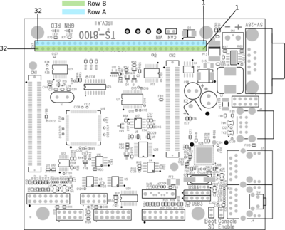
The PC/104 connector consists of two rows of pins labeled A and B, the numbering of of which is shown below. The signals for the PC-104 are generated by the MAX240 PLD located on the baseboard. It converts the MUXBUS signals from the dual 100-pin System-on-Module TS-STOCKET interface bus.
Any of the IO on this board labelled DIO_ can be controlled through manipulation of the TS-8100 registers.
You can also drive these DIO to manually manipulate the PC104 address to make peripherals usable that require a higher range of address than provided by the default address space of the MUXBUS.
| Pin
|
Name
|
Pin
|
Name
|
| A1
|
BUS_BHE#
|
B1
|
Ground
|
| A2
|
AD_07
|
B2
|
ISA_RESET
|
| A3
|
AD_06
|
B3
|
5V
|
| A4
|
AD_05
|
B4
|
AD_08
|
| A5
|
AD_04
|
B5
|
CPU_3.3V
|
| A6
|
AD_03
|
B6
|
Not connected
|
| A7
|
AD_02
|
B7
|
Not connected
|
| A8
|
AD_01
|
B8
|
Not connected
|
| A9
|
AD_D0
|
B9
|
VIN
|
| A10
|
ISA_WAIT#
|
B10
|
Ground
|
| A11
|
Ground
|
B11
|
DIO_B11
|
| A12
|
Not connected
|
B12
|
DIO_B12
|
| A13
|
Not connected
|
B13
|
ISA_LOW#
|
| A14
|
Not connected
|
B14
|
ISA_IOR#
|
| A15
|
Not connected
|
B15
|
Not connected
|
| A16
|
DIO_A16
|
B16
|
Not connected
|
| A17
|
DIO_A17
|
B17
|
AD_09
|
| A18
|
DIO_A18
|
B18
|
AD_10
|
| A19
|
DIO_A19
|
B19
|
Not connected
|
| A20
|
DIO_A20
|
B20
|
AD_12
|
| A21
|
DIO_A21
|
B21
|
ISA_IRQ7
|
| A22
|
ISA_ADD9
|
B22
|
ISA_IRQ6
|
| A23
|
ISA_ADD8
|
B23
|
ISA_IRQ5
|
| A24
|
ISA_ADD7
|
B24
|
Ground
|
| A25
|
ISA_ADD6
|
B25
|
AD_11
|
| A26
|
ISA_ADD5
|
B26
|
AD_13
|
| A27
|
ISA_ADD4
|
B27
|
AD_14
|
| A28
|
ISA_ADD3
|
B28
|
AD_15
|
| A29
|
ISA_ADD2
|
B29
|
5V
|
| A30
|
ISA_ADD1
|
B30
|
ISA 14.3 MHZ
|
| A31
|
ISA_ADD0
|
B31
|
Ground
|
| A32
|
Ground
|
B32
|
Ground
|
|
|
| WARNING:
|
Most of the pins on the PC104 bus are only 3.3V tolerant. Refer to the schematic for more details.
|
