TS-8551-socket
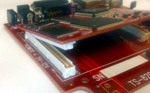
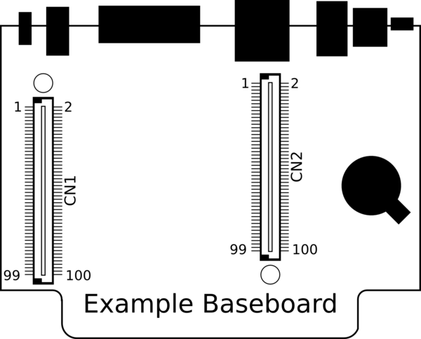
The TS-SOCKET SoM devices all use 2 high density 100 pin connectors for power and all I/O. These follow a common pinout for various external interfaces so new modules can be switched in to an application in order to lower power consumption or use a more powerful processor. The male connector is on the baseboard, and the female connector is on the SoM. The datasheet for the baseboard's male connector can be found here. Connectors can be ordered from the SoM's product page as CN-TSSOCKET-M-10 for a 10 pack, or CN-TSSOCKET-M-100 for 100 pieces, or from the vendor of your choice; the part is an FCI 61083-102402LF.

In our schematics and our table layout below, we refer to pin 1 from the male connector on the baseboard.
On the TS-8551, the entirety of both high-density connectors are broken out in to 0.1" spaced 2x25 pin headers. There are 4 of these in total, one each for CN1 odd numbered pins, CN1 even numbered pins, CN2 even numbered pins, and CN2 odd numbered pins. They are labeled on the silkscreen every 10 pins, with the first 2 and last 2 pins also being labeled.
Note that the below pinout is from the perspective of the TS-8551. However, the links for each pin will link to the relevant section in this manual. When designing a custom baseboard, it is advised to consider both the TS-8551's TS-SOCKET pinout and functions as well as the target SoM's pinout. For details on a specific SoM's interface, see that device's manual.
- ↑ 1.0 1.1 1.2 1.3 The FPGA JTAG pins are not recommended for use and are not supported.
- ↑ EXT_RESET# is an input used to reboot the CPU. Do not drive active high, use open drain.
- ↑ This is an output which can be manipulated as a GPIO. This pin can optionally be connected to control a FET to a separate 5 V rail for USB to allow software to reset USB devices.
- ↑ OFF_BD_RESET# is an output from the SoM that automatically sends a reset signal when the unit powers up or reboots. It can be connected to any IC on the base board that requires a reset.
- ↑ 5.0 5.1 This interface is for programming the on-board microcontroller of the SoM, this should be left unconnected on a baseboard.
- ↑ 6.0 6.1 6.2 6.3 The power pins should each be provided with a 5 V source.
- ↑ Connect to a 1 kohm pull down to disable Supercapacitor charging on compatible SoMs. Can be used as GPIO after boot.
- ↑ Connect to a 1 kohm pull down to enter the U-Boot shell at power on on compatible SoMs. Can be used as GPIO after boot.
- ↑ When low, overrides the microcontroller power control and enables 5 V rail on the SoM. Leave unconnected for normal use.
- ↑ 10.0 10.1 Allows the supervisory microcontroller to measure USB VBUS for the OTG port.
- ↑ Normally NC or pulled to ground via 1 kohm resistor. Optionally can be switched/jumpered to pull to 3.3 V through a 1 kohm resistor; this allows other booting options provided by SoM. Not all SoMs honor this pin.
- ↑ Pull to ground through 1 kohm resistor to boot to SD. Leave floating to boot from on-board media. Do not connect directly to ground or 3.3 V or baseboard ID will no longer function.
- ↑ 13.0 13.1 13.2 13.3 The Ethernet jack on the TS-8551 is rated for 1000Base-T operation, but is compatible with 10/100Base-TX PHYs
- ↑ 14.0 14.1 14.2 14.3 14.4 The CPU JTAG pins are not recommended for use and are not supported.
- ↑ Not output from every SoM.
- ↑ 16.0 16.1 16.2 16.3 Do not connect to the TTL interface for this UART that is present on the CN breakout pin headers. Doing so may damage the SoM or the connected hardware
