TS-9700
 | |
| Product Page | |
| Documentation | |
|---|---|
| Schematic |
Overview
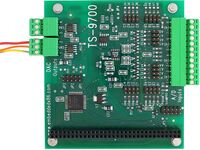
The Technologic Systems TS-9700 is a PC/104 daughter board that provides 8 channels of 12-bit Analog-to-Digital (A/D) conversion using a precision 0.2% analog reference. A single Analog Devices AD7888 chip implements the heart of the A/D subsystem. Each analog input can be individually jumper selected for one of three ranges:
 0 – 2.5 Volt
 0 – 10.0 Volt
 0 – 20 mA
The Analog-to-Digital conversion takes 9 microseconds to complete allowing up to 100K samples per second. The TS-9700 can optionally be populated with 4 channels of 12-bit digital-to-analog conversion using a 0.2% analog reference. Two Texas Instruments TLV5818 chips are used to implement the four Digital-to-Analog converter (DAC) outputs. Each DAC output has a rail-to-rail output buffer that allows a nominal 0 to 5 Volt output swing using a single 5V power supply.
Features
PC104 Interface
The TS-9700 features an 8-bit industry standard PC/104 bus that is compatible with all Technologic Systems series of SBC. The TS-9700 requires a block of 8 bytes in the I/O space. The location of the base I/O address of this block can be selected via 3 jumpers as shown in Table 1 This allows for multiple TS-9700 boards to be used in a single system. A Xilinx programmable logic device (PLD) is used to decode the Base I/O address. This allows for a great amount of flexibility in the standard product and allows for custom configurations if they are necessary. Call Technologic Systems for more details.
IO Address
| JP1 | JP2 | JP3 | IO Address |
|---|---|---|---|
| Off | Off | Off | 0x160 |
| On | Off | Off | 0x168 |
| Off | On | Off | 0x180 |
| On | On | Off | 0x188 |
| Off | Off | On | 0x250 |
| On | Off | On | 0x258 |
| Off | On | On | 0x268 |
| On | On | On | 0x268 |
A/D Acquisition Cycles
Any write to the A/D command register at offset 0x0 will initiate an analog-to-digital conversion with the 12-bit result being stored into the A/D LSB and A/D MSB registers. Bits 0-2 select the channel (0-7) to be converted. The result will not be available for approximately 9 microseconds (for single acquisition mode) after the command register has been written. This delay is due to the acquisition time required by the AD7888 chip. The 12-bit result can be read in a single 16-bit word cycle or as two byte reads. Since there are only 12-bits for each acquisition, the upper 4-bits of the A/D MSB register are always read as zeros. The A/D command register should be polled (read cycles only) until bit 7 is set high before attempting to read the A/D result. Bit 7 of the A/D command register is a read-only status bit that is a logic 0 while an A/D acquisition is in progress.
The TS-9700 allows two different types of acquisitions, single cycle and double cycle modes. The single cycle mode (Bit 4 = logic 1) takes 9 microseconds to complete while a double cycle requires 18 microseconds. Due to the design of the AD7888 chip, it is not possible to select the channel to convert and also convert the selected channel in a single 9 microsecond cycle. The AD7888 uses a pipelined architecture where the channel being converted is determined by the value of bits 0-2 for the previous cycle. This mode can be used for the highest sampling rate possible, but if you need to sample random channels, it is simpler to use the double cycle mode (Bit 4 = logic 0). In the double cycle mode, the Xilinx PLD state machine does two complete acquisitions, with the first used to get the desired channel into the AD7888 chip, and the second cycle then does the acquisition on the correct channel.
Digital-to-Analog Converter
The TS-9700 uses two Texas Instruments TLV5618 chips to implement 4 channels of 12-bit digital-to-analog conversion. Each DAC output has a rail-to-rail output buffer that allows a nominal 0 to 5 Volt output swing using a single 5V power supply. The same precision 2.5V reference is used for both the A/D and DAC functions. The TLV5618 has an internal fixed gain stage of 2 that allows 0-5V output operation using the 2.5V precision reference. This equation determines the output voltage: 5.000 x (code) / 4096 Where code is the 12-bit binary value (0-4095 decimal) loaded into the DAC. The suggested load impedance on the TLV5618 should not be lower than 2 kohms. The TLV5618 can sink or source in excess of 5 mA, but when operating within .2V of either supply rail (5V and GND), the output will clipped. The TLV5618 chip is being powered by the raw 5V power to the PC/104 stack of boards. Due to limitations in the output amplifier in the TLV5618, it is helpful to run this supply voltage at the high end of its operational range. For example a 5.25V power supply voltage will allow the TLV5618 to reach its full-scale output voltage.
If running at less than 5V supply voltage, the TLV5618 chip will not lose any accuracy except near the top end of its output dynamic range. When the output is driven within 0.2V of the top supply rail, it will begin to clamp, and its linearity will not meet specifications.
The DAC register is a 16-bit register located at I/O location Base + 4 and Base + 5. These registers can be read or written. These registers can be written as a single 16-bit word cycle (at Base + 4), or two byte write cycles can be used provided the lower byte is written first. Anytime the Base + 5 register is written, a DAC update cycle occurs. Table 4 describes the function of each bit this register. Any write to the DAC MSB register will initiate a DAC cycle with the lower 12-bits being the value written into one of the four DAC channels or into a buffer register. Bits 14,15 select the DAC channel (1-4) to be written into. Bit 13 allows the DAC value to be written into a Buffer register inside the TLV5617 chip. This buffer register acts as temporary holding register.
This special cycle is implemented to allow for a simultaneous update of two DAC channels. For example, if the Bit 13 is set and Bit 15 is clear, then the DAC cycle will update the buffer in the TLV5617, but will not change any analog output. Then when a DAC cycle is run writing to Channel 2, Channel 1 will be updated with the holding register value. Both Channel 1 and Channel 2 analog outputs will change at exactly the same time. Channels 3 and 4 can also implement this simultaneous update in the same manner except Bit 15 must be set for the buffer write cycle. If simultaneous updates are not required, always leave bit 13 clear and simply select one of the four channels with bits 14 and 15. Bit 12 set selects a fast settling time of about 3 microseconds, while Bit 12 clear will select a slower 10 microseconds. Consult the TLV5618 data sheet for details. When using the slow settling mode, the analog output has a slighter greater current sink and source capability. So this may be more desirable than the faster settling time.
| Note: | The DAC is an optional feature and requires you to order the board with OP-DAC4 to use this functionality. |
Jumper Selection for A/D Converter
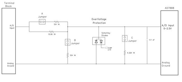
The TS-9700 uses the Analog Devices AD7888 chip to implement 8 channels of 12-bit analog-to-digital conversion. The AD7888 chip always requires a 0-2.5V input range for proper operation. The TS-9700 has 3 jumpers per A/D channel to select several different modes of operation. Please refer to Figure 1. All jumpers are labeled A, B, or C followed by the channel number. For example, for A/D channel #3, the jumpers are A3, B3, and C3.

To select a 0-10V input range for a particular channel, only Jumper “C” should be installed. This causes the 4.32K and 13.0K resistors to form a 4:1 voltage divider that divides the input voltage down to 0-2.5V for the AD7888. The AD7888 does not introduce any errors due to loading, since the input impedance is several megaohms. In this mode, the bandwidth of the channel is limited to 500 Hz due to the low pass filter formed by the 0.1 uF capacitor and the nominal 3.3 Kohms source impedance in the resistive divider. To select a 0-2.5V range, the jumpers can be positioned in two different ways. If no jumpers are installed, a low pass filter is formed by the 13.0K resistor and the 0.1 uF capacitor with a corner frequency of 120 Hz. If only Jumper “A” is installed, a 0-2.5V range is still selected, but the input resistor is lowered to 124 ohms resulting in a 10 KHz low pass filter. In both of these jumper configurations, the 0-2.5V range has the advantage of a direct conversion with no resistor dividers to introduce any errors due to resistor tolerance. The 0-2.5V range also has the advantage of an input impedance of several megaohms, compared to 17 kohm for the 0-10V range.
To select the 0-20 mA range, Jumper “A” and Jumper “B” both must be installed. A 20 mA current will produce 2.400V (20 mA x 124 ohms) into the AD7888 chip.
Monitoring 5V
The TS-9700 has two pads labeled JP5 near the PC/104 bus connector. If these pads are shorted, the 5V supply is connected to A/D channel # 7. This may be useful for monitoring the power supplied to the PC/104 stack. If using this feature it is required that jumper C7 be installed, and that jumpers B7 and A7 not be installed, so that A/D channel #7 is in a 0-10V range.
Reference Voltage
The TS-9700 uses a Texas Instruments LT1009 chip as the reference voltage for both the A/D converter and the DAC. This chip provides a 0.2% accurate 2.5V reference voltage. If more accuracy is required, it is always possible to calibrate any channel with an external precision input to obtain more accuracy. This same technique can be used to eliminate any error introduced by resistor tolerances when using the 0-10V range or the 0-20 mA range.
Register Map
| Offset | Bits | Access | Description |
|---|---|---|---|
| 0x0 | 7 | Read/Write | A/D Acquisition Status (ready = 1) |
| 5:6 | Read-Only | Reserved | |
| 4 | Read/Write | Single Acquisition Mode (single = 1) | |
| 3 | Read Only | Reserved | |
| 0:2 | Read/Write | Selects A/D channel | |
| 0x1 | 7-0 | Read/Write | ID Register (0x97) |
| 0x2 | 7:0 | Read-Only | A/D LSB |
| 0x3 | 7:0 | Read-Only | A/D MSB (upper 4 bits = 0) |
| 0x4 | 7:0 | Read/Write | Value to DAC |
| 0x5 | 6:7 | Read/Write | DAC Select
00 = Channel #1 |
| 5 | Read/Write | Write to buffer only | |
| 4 | Read/Write | Fast DAC mode | |
| 3:0 | Read/Write | Value to DAC (Upper bits) | |
| 0x6 | 7:0 | Read-Only | DAC Status (bit 7 = Ready) |
| 0x7 | 7:0 | Read-Only | Reserved |
Connectors
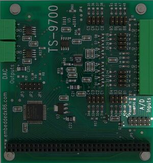
12 pin terminal block
The 12 pin header brings out A/D and ground channels. You can find a mating connector from On Shore Technologies as "OSTTJ1211530".
| Pin | Function |
|---|---|
| 1 | ADC Channel 1 |
| 2 | Ground |
| 3 | ADC Channel 2 |
| 4 | ADC Channel 3 |
| 5 | Ground |
| 6 | ADC Channel 4 |
| 7 | ADC Channel 5 |
| 8 | Ground |
| 9 | ADC Channel 6 |
| 10 | ADC Channel 7 |
| 11 | Ground |
| 12 | ADC Channel 8 |
10 Pin Header
Along with the 12 pin terminal block, the ADC channels are also brought out on the 10 pin header pictured on the right. These pins are 0.100" pitch.

|
|
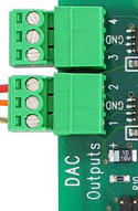
2x 3 Pin Terminal Bocks
The two 3 pin terminal blocks bring out the DAC channels.
You can find a compatible mating connector from On Shore Technologies as "OSTTJ0311530".
FCC Advisory
This equipment generates, uses, and can radiate radio frequency energy and if not installed and used properly (that is, in strict accordance with the manufacturer's instructions), may cause interference to radio and television reception. It has been type tested and found to comply with the limits for a Class A digital device in accordance with the specifications in Part 15 of FCC Rules, which are designed to provide reasonable protection against such interference when operated in a commercial environment. Operation of this equipment in a residential area is likely to cause interference, in which case the owner will be required to correct the interference at his own expense.
If this equipment does cause interference, which can be determined by turning the unit on and off, the user is encouraged to try the following measures to correct the interference:
Reorient the receiving antenna. Relocate the unit with respect to the receiver. Plug the unit into a different outlet so that the unit and receiver are on different branch circuits. Ensure that mounting screws and connector attachment screws are tightly secured. Ensure that good quality, shielded, and grounded cables are used for all data communications. If necessary, the user should consult the dealer or an experienced radio/television technician for additional suggestions. The following booklets prepared by the Federal Communications Commission (FCC) may also prove helpful:
How to Identify and Resolve Radio-TV Interference Problems (Stock No. 004-000-000345-4) Interface Handbook (Stock No. 004-000-004505-7) These booklets may be purchased from the Superintendent of Documents, U.S. Government Printing Office, Washington, DC 20402.
Limited Warranty
See our Terms and Conditions for more details.
Usage with 3rd party devices
Please note that while efforts are made to follow the PC/104 specification this peripheral is not tested with third party SBCs or connected peripherals. This card is not guaranteed to operate as intended when third party PC104 peripherals or SBCs are connected.
