TS-7250-V3 LCD Header: Difference between revisions
From embeddedTS Manuals
No edit summary |
No edit summary |
||
| (4 intermediate revisions by 2 users not shown) | |||
| Line 1: | Line 1: | ||
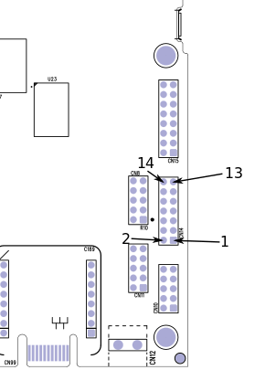
The LCD header is a 0.1" pitch 2x7 header including GPIO. This is designed around compatibility with the HD44780 LCD controller which includes our [https://www. | The LCD header is a 0.1" pitch 2x7 header including GPIO. This is designed around compatibility with the HD44780 LCD controller which includes our [https://www.embeddedTS.com/parts/LCD-LED LCD-LED]. The LCD Data pins (7-14) are 5V tolerant. These will output up to 3.3V, and the remaining control IO and PWM are 3.3V tolerant. The TS-7250-V3 Debian images include a command [https://github.com/embeddedTS/ts7100-utils/blob/master/src/lcdmesg.c lcdmesg]. This can be used to write to our [https://www.embeddedTS.com/parts/LCD-LED LCD-LED] display. | ||
For example, this would write to the display: | |||
<source lang=bash> | |||
lcdmesg "line 1" "line 2" | |||
# Messages can also be piped to lcdmesg: | |||
echo -e "line 1\nline 2\n" | lcdmesg | |||
</source> | |||
For example, running: | |||
<source lang=bash> | |||
lcdmesg Technologic Systems | |||
</source> | |||
will display: | |||
[[File:LCD LED example.jpg|500px]] | |||
Pin 4, the LCD_BIAS pin, is used to set the contrast on the LCD. | |||
<source lang=bash> | |||
tshwctl --address 0x1c --poke16 0x0 # Writes minimum | |||
tshwctl --address 0x1c --poke16 0xf # Writes maximum | |||
</source> | |||
{| | {| | ||
| Line 9: | Line 30: | ||
|- | |- | ||
! Pin | ! Pin | ||
! IO Type | |||
! Signal | ! Signal | ||
|- | |- | ||
| 1 | | 1 | ||
| | |||
| [[#Board Rails|5V]] | | [[#Board Rails|5V]] | ||
|- | |- | ||
| 2 | | 2 | ||
| | |||
| GND | | GND | ||
|- | |- | ||
| 3 | | 3 | ||
| LCD_RS [[#GPIO|GPIO | | [[#IO specifications|CPU 3.3V]] | ||
| LCD_RS [[#GPIO|GPIO Chip 20a4000.gpio IO 21]] | |||
|- | |- | ||
| 4 | | 4 | ||
| | | [[#IO specifications|CPU 3.3V]] | ||
| LCD_BIAS <ref>PWM duty cycle controlled by [[#FPGA Syscon|FPGA Syscon reg 0x1c]]. This may need to be tuned depending on the environment or altitude where the display is used.</ref> | |||
|- | |- | ||
| 5 | | 5 | ||
| LCD_EN [[#GPIO|GPIO | | [[#IO specifications|CPU 3.3V]] | ||
| LCD_EN [[#GPIO|GPIO Chip 50004010.fpga_gpio IO 20]] | |||
|- | |- | ||
| 6 | | 6 | ||
| LCD_WR [[#GPIO|GPIO | | [[#IO specifications|CPU 3.3V]] | ||
| LCD_WR [[#GPIO|GPIO Chip 50004010.fpga_gpio IO 19]] | |||
|- | |- | ||
| 7 | | 7 | ||
| LCD D1 [[#GPIO|GPIO | | [[#IO specifications|CPU 3.3V+QS3861]] | ||
| LCD D1 [[#GPIO|GPIO Chip 20a4000.gpio IO 9]] | |||
|- | |- | ||
| 8 | | 8 | ||
| LCD D0 [[#GPIO|GPIO | | [[#IO specifications|CPU 3.3V+QS3861]] | ||
| LCD D0 [[#GPIO|GPIO Chip 50004010.fpga_gpio IO 10]] | |||
|- | |- | ||
| 9 | | 9 | ||
| LCD D3 [[#GPIO|GPIO | | [[#IO specifications|CPU 3.3V+QS3861]] | ||
| LCD D3 [[#GPIO|GPIO Chip 50004010.fpga_gpio IO 11]] | |||
|- | |- | ||
| 10 | | 10 | ||
| LCD D2 [[#GPIO|GPIO | | [[#IO specifications|CPU 3.3V+QS3861]] | ||
| LCD D2 [[#GPIO|GPIO Chip 50004010.fpga_gpio IO 12]] | |||
|- | |- | ||
| 11 | | 11 | ||
| LCD D5 [[#GPIO|GPIO | | [[#IO specifications|CPU 3.3V+QS3861]] | ||
| LCD D5 [[#GPIO|GPIO Chip 50004010.fpga_gpio IO 15]] | |||
|- | |- | ||
| 12 | | 12 | ||
| LCD D4 [[#GPIO|GPIO | | [[#IO specifications|CPU 3.3V+QS3861]] | ||
| LCD D4 [[#GPIO|GPIO Chip 50004010.fpga_gpio IO 16]] | |||
|- | |- | ||
| 13 | | 13 | ||
| LCD_D7 [[#GPIO|GPIO | | [[#IO specifications|CPU 3.3V+QS3861]] | ||
| LCD_D7 [[#GPIO|GPIO Chip 50004010.fpga_gpio IO 17]] | |||
|- | |- | ||
| 14 | | 14 | ||
| LCD_D6 [[#GPIO|GPIO | | [[#IO specifications|CPU 3.3V+QS3861]] | ||
| LCD_D6 [[#GPIO|GPIO Chip 50004010.fpga_gpio IO 18]] | |||
|} | |} | ||
| | | | ||
| Line 58: | Line 94: | ||
<References /> | <References /> | ||
Latest revision as of 10:10, 9 April 2024
The LCD header is a 0.1" pitch 2x7 header including GPIO. This is designed around compatibility with the HD44780 LCD controller which includes our LCD-LED. The LCD Data pins (7-14) are 5V tolerant. These will output up to 3.3V, and the remaining control IO and PWM are 3.3V tolerant. The TS-7250-V3 Debian images include a command lcdmesg. This can be used to write to our LCD-LED display.
For example, this would write to the display:
lcdmesg "line 1" "line 2"
# Messages can also be piped to lcdmesg:
echo -e "line 1\nline 2\n" | lcdmesg
For example, running:
lcdmesg Technologic Systems
will display:
Pin 4, the LCD_BIAS pin, is used to set the contrast on the LCD.
tshwctl --address 0x1c --poke16 0x0 # Writes minimum
tshwctl --address 0x1c --poke16 0xf # Writes maximum
| Signals | Pin Layout | |||||||||||||||||||||||||||||||||||||||||||||
|---|---|---|---|---|---|---|---|---|---|---|---|---|---|---|---|---|---|---|---|---|---|---|---|---|---|---|---|---|---|---|---|---|---|---|---|---|---|---|---|---|---|---|---|---|---|---|
|
- ↑ PWM duty cycle controlled by FPGA Syscon reg 0x1c. This may need to be tuned depending on the environment or altitude where the display is used.

