TS-8100 PC104: Difference between revisions
From embeddedTS Manuals
No edit summary |
(Change from Macrocontroller to SoM) |
||
| (One intermediate revision by one other user not shown) | |||
| Line 1: | Line 1: | ||
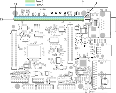
The PC | The PC/104 connector consists of two rows of pins labeled A and B, the numbering of of which is shown below. The signals for the PC-104 are generated by the MAX240 PLD located on the baseboard. It converts the MUXBUS signals from the dual 100-pin System-on-Module TS-STOCKET interface bus. | ||
Any of the IO on this board labelled DIO_ can be controlled through manipulation of the [[#TS- | Any of the IO on this board labelled DIO_ can be controlled through manipulation of the [[#TS-81XX Register Map|TS-8100 registers]]. | ||
You can also drive these DIO to manually manipulate the PC104 address to make peripherals usable that require a higher range of address than provided by the default address space of the MUXBUS. | You can also drive these DIO to manually manipulate the PC104 address to make peripherals usable that require a higher range of address than provided by the default address space of the MUXBUS. | ||
Latest revision as of 11:23, 13 June 2023
The PC/104 connector consists of two rows of pins labeled A and B, the numbering of of which is shown below. The signals for the PC-104 are generated by the MAX240 PLD located on the baseboard. It converts the MUXBUS signals from the dual 100-pin System-on-Module TS-STOCKET interface bus.
Any of the IO on this board labelled DIO_ can be controlled through manipulation of the TS-8100 registers.
You can also drive these DIO to manually manipulate the PC104 address to make peripherals usable that require a higher range of address than provided by the default address space of the MUXBUS.
| WARNING: | Most of the pins on the PC104 bus are only 3.3V tolerant. Refer to the schematic for more details. |
