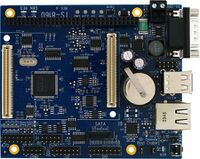
TS-8160-4200
 | |
| Released Mar. 2011 | |
| Product Page | |
| Documentation | |
|---|---|
| Schematic | |
| Mechanical Drawing |
Overview
The TS-8160 is a TS-SOCKET baseboard that provides an upgrade path for Technologic Systems TS-7260 and TS-7800 products. This board accepts any TS-4xxx macrocontroller. It interfaces to the macrocontroller via two TS-SOCKET standard 100-pin connectors and brings out the various ports to industry standard connectors. The TS-8160 is compatible with the TS-ENC720 enclosure.
TS-4200
See the TS-4200 page for functionality regarding the CPU, FPGA, and OS.

|
Atmel AT91SAM9G20 400MHz ARM9 |
Getting Started
Before attempting to apply power to the baseboard, perform the following steps while taking proper static discharge precautions
- Place the TS-8160 base board on a firm non-conductive surface.
- Place the COM1 "Console Enable" jumper in the console position so the debug port is brought out.
- Carefully, insert the macrocontroller daughterboard by aligning and pressing evenly and firmly onto the pair of mating connectors
- Connect the console serial terminal cable
- Connect the Ethernet cable is applicable.
- Apply power
- Monitor the TS-SOCKET SBC using a terminal emulator connected to the serial console port to verify that the board is operating properly
See the TS-4200 page for more details on dealing with the functionality of the macrocontroller.
Features
Software
The TS-8160 baseboards contains no processor or memory, and therefore do not have software on the board. All required software is supplied and executes on the selected Macrocontroller. There is a specific utility called ts8160ctl that runs on the attached Macrocontroller when paired with the TS-8160, and is used to set the sleep mode and sleep mode timing. There is no other software directly associated with the TS-8100/8160. The ts8160ctl is available here.
Register Map
All of these registers are intended for 16 bit access. You can find this range at 0x30000400. You must first set the MUXBUS configuration register before accessing this range. For example, to read the board ID:
peekpoke 16 0x30000020 0x181
peekpoke 16 0x30000400
| Offset | Bits | Name | Access | Description |
|---|---|---|---|---|
| 0x0 | 15:0 | Board ID | Read Only | Returns '0x8100' |
| 0x2 | 3:0 | PLD revision | Read Only | |
| 7:4 | LCD Contrast | Read/Write | ||
| 8 | USB Reset | Read/Write | Allows you to reset the USB hub | |
| 9 | ISA Reset | Read/Write | ||
| 10 | Enable Oscillator | Read/Write | ||
| 11 | Enable RS-232 | Read/Write | ||
| 12 | Enable LCD Power | Read/Write | ||
| 13 | CAN1 Standby | Read/Write | ||
| 14 | CAN2 Standby | Read/Write | ||
| 15 | LCD Contrast Enable | Read/Write | ||
| 0x4 | 7:0 | Odd numbered pins 15:1 | Read/Write | Output data on the DIO header |
| 13:8 | PC104 pins A21:A16 | Read/Write | Output data on PC104 header | |
| 15:14 | PC104 pins B12:B11 | Read/Write | Output data on PC104 header | |
| 0x6 | 7:0 | Pins 14-7 data | Read Only | LCD data lines output data |
| 8 | LCD Write/Read (pin 6) | Read/Write | LCD Header pin 6 output data | |
| 9 | LCD Register Select (pin 3) | Read/Write | LCD Header pin 3 output data | |
| 10 | LCD Enable (pin 5) | Read/Write | LCD Header pin 5 output data | |
| 11 | AVR MOSI | Read/Write | ||
| 12 | AVR SCLK | Read/Write | ||
| 13 | AVR RESET | Read/Write | ||
| 14:15 | Reserved | N/A | ||
| 0x8 | 7:0 | DIO data direction (odd pins 15:1) | Read/Write | DIO Header data direction |
| 13:8 | PC104 pins A21:A16 | Read/Write | PC104 GPIO data direction | |
| 15:14 | PC104 pins B12:B11 | Read/Write | PC104 GPIO data direction | |
| 0xa | 7:0 | Pins 14-7 direction | Read Only | Set the data direction for the LCD GPIO |
| 8 | LCD Write/Read (pin 6) | Read/Write | Set the LCD Header pin 6 direction | |
| 9 | LCD Register Select (pin 3) | Read/Write | Set the LCD Header pin 3 direction | |
| 10 | LCD Enable (pin 5) | Read/Write | Set the LCD Header pin 5 direction | |
| 0xc | 7:0 | DIO Input Data (odd pins 15:1) | Read/Write | DIO Header input data |
| 13:8 | PC104 pins A21:A16 | Read/Write | PC104 GPIO input data | |
| 15:14 | PC104 pins B12:B11 | Read/Write | PC104 GPIO input data | |
| 0xe | 7:0 | Pins 14-7 data | Read Only | LCD Header input data |
| 8 | LCD Write/Read (pin 6) | Read/Write | For selecting between reads/writes | |
| 9 | LCD Register Select (pin 3) | Read/Write | Select between data and instruction registers | |
| 10 | LCD Enable (pin 5) | Read/Write | Toggles the LCD functionality | |
| 11 | AVR MISO | Read/Write | ||
| 15:12 | Reserved | N/A |