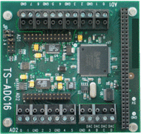
TS-ADC16: Difference between revisions
(Added address jumpers.) |
(→Jumpers: Added SBC and IRQ jumper selection tables.) |
||
| Line 196: | Line 196: | ||
|on | |on | ||
|0x160 | |0x160 | ||
|} | |||
{|class = "wikitable" | |||
|+SBC Mode | |||
!JP4 | |||
!Mode | |||
|- | |||
|on | |||
|ARM | |||
|- | |||
|off | |||
|x86 | |||
|} | |||
{|class="wikitable" | |||
|+IRQ Selection | |||
!JP4 | |||
!IRQ | |||
|- | |||
|on | |||
|IRQ 7 | |||
|- | |||
|off | |||
|IRQ 6 | |||
|} | |} | ||
Revision as of 15:35, 12 September 2012
 | |
| Product Page | |
| Documentation | |
|---|---|
| Schematic | |
| Mechanical Drawing | |
| FTP Path | |
| ADC Datasheet | |
| DAC Datasheet |
OVERVIEW
The TS-ADC16 is a 8-bit (16-bit in ARM mode) PC/104 peripheral board (standard format) that provides 16 channels of 16-bit analog to digital conversion (ADC or A/D converter) with internal 512x16bit RAM-FIFO. In addition, it provides 4 channels of 12-bit digital to analog conversion (DAC), 4 16-bit counters, 4 digital inputs and 1 digital output. It is a strong solution for data acquisition, measurement, control and analog interface applications. Features include:
| Features |
|---|
| Two LTC1859 ADC chips |
| 16 channels 16-bit ADC |
| ADC Sampling rate up to 2x100ksps |
| Takes 2 ADC samples simultaneously |
| 4 different ADC ranges |
| 512x16bit RAM-FIFO for ADC data |
| 4 digital inputs - 0 to 5V |
| 1 digital output - 0 to 3.3V/50mA |
| 4 12-bit DAC channels |
| 4 16-bit counters |
| Jumper selectable I/O an IRQ |
| PC/104 Dimensions 3.6 x 3.8 inches |
Headers and Pins
The TS-ADC16 has one jumper block (JP), two AD headers (AD1, AD2), and two banks of screw terminals. The tables below describe each of these features.
| gnd | gnd | gnd | gnd | gnd | gnd | gnd | gnd | gnd | gnd | gnd | gnd | gnd |
|---|---|---|---|---|---|---|---|---|---|---|---|---|
| PIN-02 | PIN-04 | PIN-06 | PIN-08 | PIN-10 | PIN-12 | PIN-14 | PIN-16 | PIN-18 | PIN-20 | PIN-22 | PIN-24 | PIN-26 |
| *PIN-01 | PIN-03 | PIN-05 | PIN-07 | PIN-09 | PIN-11 | PIN-13 | PIN-15 | PIN-17 | PIN-19 | PIN-21 | PIN-23 | PIN-25 |
| AD1-0 | AD1-1 | AD1-2 | AD1-3 | AD1-4 | AD1-5 | AD1-6 | AD1-7 | D-OUT | D-IN0 | D-IN1 | D-IN2 | D-IN3 |
| gnd | gnd | gnd | gnd | gnd | gnd | gnd | gnd | gnd | gnd | gnd | gnd | gnd |
|---|---|---|---|---|---|---|---|---|---|---|---|---|
| PIN-02 | PIN-04 | PIN-06 | PIN-08 | PIN-10 | PIN-12 | PIN-14 | PIN-16 | PIN-18 | PIN-20 | PIN-22 | PIN-24 | PIN-26 |
| *PIN-01 | PIN-03 | PIN-05 | PIN-07 | PIN-09 | PIN-11 | PIN-13 | PIN-15 | PIN-17 | PIN-19 | PIN-21 | PIN-23 | PIN-25 |
| AD1-0 | AD1-1 | AD1-2 | AD1-3 | AD1-4 | AD1-5 | AD1-6 | AD1-7 | GND | DAC-A | DAC-B | DAC-C | DAC-D |
Pin 1 on both tables can be identified by a small white dot silkscreened on the PCB.
Jumpers
The jumper block controls three functions: PC104 Address setting (JP1, JP2), ARM SBC mode (JP3), and IRQ Selection (JP4).
| jp1 | jp2 | Address |
|---|---|---|
| off | off | 0x100 |
| on | off | 0x120 |
| off | on | 0x140 |
| on | on | 0x160 |
| JP4 | Mode |
|---|---|
| on | ARM |
| off | x86 |
| JP4 | IRQ |
|---|---|
| on | IRQ 7 |
| off | IRQ 6 |